PCB Via Plugging Solutions: A Comprehensive Guide
Introduction
Printed Circuit Boards (PCBs) are essential components in modern electronics, enabling the interconnection of various electronic parts. Vias—small holes drilled into PCBs—play a crucial role in establishing electrical connections between different layers. However, via clogging (or via plugging) is a common issue that can lead to manufacturing defects, poor solderability, and reduced reliability. This article explores the causes of via clogging, its impact on PCB performance, and detailed solutions to prevent and resolve this problem.
1. Understanding Via Clogging in PCBs
1.1 What is Via Clogging?
Via clogging occurs when conductive or non-conductive materials block the via hole, preventing proper plating, solder flow, or electrical connectivity. This can happen during manufacturing, assembly, or even in field operation due to environmental factors.
1.2 Causes of Via Clogging
Several factors contribute to via clogging, including:
- Solder Mask Intrusion: Excessive solder mask can seep into vias during application.
- Poor Plating: Incomplete copper plating inside the via can trap residues.
- Contamination: Dust, debris, or chemical residues from fabrication processes.
- Improper Drilling: Incorrect drill size or misalignment can lead to partial blockage.
- Thermal Stress: Repeated heating and cooling cycles may cause material expansion, closing vias.
- Ink or Paste Residues: Stencil printing or solder paste application errors.
1.3 Consequences of Via Clogging
- Electrical Failures: Open or intermittent connections.
- Soldering Issues: Poor solder wetting leading to weak joints.
- Signal Integrity Problems: Increased impedance or signal loss in high-frequency circuits.
- Reduced Reliability: Higher risk of thermal and mechanical failures.
2. Solutions for Preventing and Resolving Via Clogging
To mitigate via clogging, manufacturers and designers employ various techniques. Below are the most effective solutions:
2.1 Via Plugging with Epoxy Resin
Epoxy resin is a common material used to fill vias, providing mechanical strength and preventing solder wicking.
- Process:
- Clean the via to remove contaminants.
- Apply epoxy resin using a syringe or vacuum filling.
- Cure the epoxy at high temperature.
- Advantages:
- Prevents solder migration.
- Enhances thermal and mechanical stability.
- Disadvantages:
- Requires precise application to avoid air bubbles.
- May increase fabrication costs.
2.2 Conductive Via Plugging (Silver or Copper Paste)
For vias requiring electrical continuity, conductive pastes (silver or copper-filled) are used.
- Process:
- Fill the via with conductive paste.
- Cure under controlled conditions.
- Advantages:
- Maintains electrical connectivity.
- Suitable for high-current applications.
- Disadvantages:
- Higher cost than non-conductive fillers.
- Potential for oxidation over time.
2.3 Solder Mask Plugging
Solder mask plugging is a cost-effective method where liquid photoimageable solder mask (LPI) fills the via.
- Process:
- Apply LPI solder mask over the via.
- Expose to UV light to cure.
- Advantages:
- Low-cost solution.
- Compatible with standard PCB processes.
- Disadvantages:
- Not suitable for deep vias.
- May shrink during curing, leaving voids.
2.4 Electroplating and Copper Filling
For high-reliability PCBs, electroplating ensures complete via coverage.
- Process:
- Electroless copper deposition.
- Electroplating to build up copper thickness.
- Advantages:
- Ensures strong electrical connections.
- Reduces thermal resistance.
- Disadvantages:
- Complex process requiring precise control.
- Higher manufacturing costs.
2.5 Laser Drilling and Cleaning
For clogged vias, laser ablation can remove blockages.
- Process:
- Use a laser to vaporize the clogging material.
- Clean residues with chemical etching.
- Advantages:
- Precise and non-contact method.
- Effective for small, high-density vias.
- Disadvantages:
- Expensive equipment required.
- Risk of damaging surrounding materials.
2.6 Vacuum-Assisted Filling
Ensures complete via filling by removing trapped air.
- Process:
- Place PCB in a vacuum chamber.
- Inject filling material under reduced pressure.
- Advantages:
- Eliminates voids.
- Improves reliability.
- Disadvantages:
- Slower process.
- Requires specialized equipment.
2.7 Design Best Practices to Prevent Via Clogging
- Via Size Optimization: Larger vias (≥0.3mm) are less prone to clogging.
- Aspect Ratio Control: Keep via depth-to-diameter ratio below 8:1.
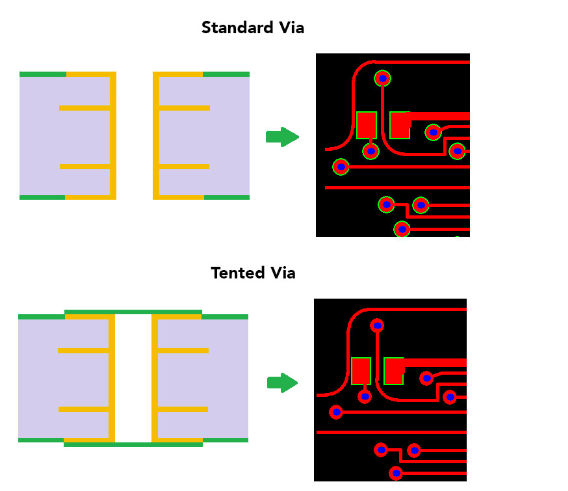
- Tented Vias: Covering vias with solder mask prevents contamination.
- Via-in-Pad Design: Use filled and capped vias for BGA and fine-pitch components.
3. Case Studies: Successful Via Clogging Solutions
3.1 High-Density Interconnect (HDI) PCBs
A smartphone manufacturer faced via clogging in microvias (0.1mm diameter). Implementing laser cleaning and vacuum-assisted epoxy filling reduced defect rates by 90%.
3.2 Automotive Electronics
An automotive PCB supplier used conductive silver paste to plug vias in engine control units, ensuring reliable connections under high-temperature conditions.
3.3 Aerospace Applications
A defense contractor employed copper electroplating for via filling in avionics PCBs, meeting stringent reliability standards.
4. Future Trends in Via Plugging Technology
- Nanomaterial Fillers: Graphene-enhanced pastes for better conductivity.
- 3D-Printed Vias: Additive manufacturing for customized via structures.
- AI-Based Inspection: Machine learning for detecting and preventing clogging defects.
5. Conclusion
Via clogging is a critical challenge in PCB manufacturing, but multiple solutions exist depending on application requirements. Epoxy filling, conductive pastes, solder mask plugging, and advanced laser techniques each offer unique benefits. By combining proper design practices with advanced manufacturing methods, PCB reliability can be significantly improved.
Key Takeaways:
- Prevention is better than cure: Optimize via design early.
- Choose the right filling method based on electrical and mechanical needs.
- Inspect and test filled vias to ensure quality.
By implementing these solutions, manufacturers can enhance PCB performance, reduce defects, and extend product lifespan.