High-Voltage Components in PCB Design: Key Considerations and Best Practices
Introduction
Printed Circuit Boards (PCBs) are essential in modern electronics, serving as the backbone for electrical connections in devices ranging from consumer electronics to industrial machinery. When designing PCBs for high-voltage applications, engineers must carefully consider the selection and placement of high-voltage components to ensure safety, reliability, and performance.
High-voltage PCBs (typically operating above 100V) require special design considerations to prevent arcing, leakage currents, and insulation breakdown. This article explores the key aspects of high-voltage components in PCB design, including material selection, layout strategies, and testing methods.
1. Understanding High-Voltage PCB Components
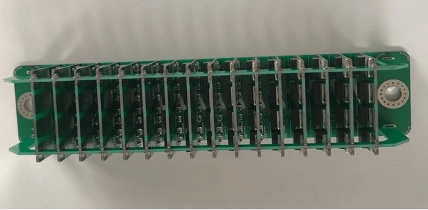
High-voltage PCBs incorporate components designed to handle elevated electrical potentials without failure. These components include:
1.1 Resistors
High-voltage resistors must withstand significant voltage gradients without breakdown. Thick-film and carbon-composition resistors are commonly used due to their high voltage ratings (up to several kV).
1.2 Capacitors
High-voltage capacitors store and regulate energy in circuits. Ceramic and film capacitors (polypropylene or polyester) are preferred for their high dielectric strength.
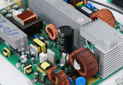
1.3 Transformers and Inductors
These components manage voltage conversion and isolation in high-voltage circuits. Proper insulation and core material selection (e.g., ferrite) are crucial.
1.4 Diodes and Thyristors
High-voltage diodes and thyristors (such as SCRs) handle switching and rectification in power electronics. Silicon carbide (SiC) and gallium nitride (GaN) devices are increasingly used for their high breakdown voltages.
1.5 Insulators and Isolation Components
Materials like polyimide, PTFE, and ceramic substrates provide necessary insulation to prevent arcing between traces.
2. PCB Material Selection for High-Voltage Applications
The choice of PCB substrate significantly impacts high-voltage performance. Key considerations include:
2.1 Dielectric Strength
The substrate must resist electrical breakdown. Common materials:
- FR4: Standard material, suitable for low to medium voltages (up to ~500V).
- Polyimide: Higher thermal stability and dielectric strength.
- Rogers & Ceramic Substrates: Excellent for RF and high-voltage applications.
2.2 Tracking Resistance
High-voltage PCBs must prevent conductive paths (tracking) due to contamination or moisture. Materials with high Comparative Tracking Index (CTI) are preferred.
2.3 Thermal Management
High voltages generate heat, requiring substrates with good thermal conductivity (e.g., metal-core PCBs or ceramic-filled laminates).
3. High-Voltage PCB Layout Design
Proper PCB layout is critical to avoid arcing, crosstalk, and EMI. Key strategies include:
3.1 Creepage and Clearance
- Creepage Distance: The shortest path along the surface between conductors. Increased spacing prevents surface arcing.
- Clearance Distance: The shortest air gap between conductors. IPC-2221 standards provide guidelines based on voltage levels.
3.2 Trace Width and Spacing
- Wider traces reduce resistance and heat buildup.
- Increased spacing minimizes risk of arcing (e.g., 0.5mm per 100V for internal layers).
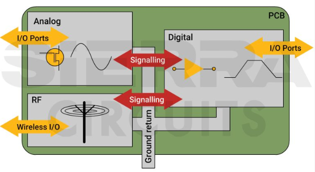
3.3 Grounding and Shielding
- Proper grounding reduces noise and prevents floating high-voltage nodes.
- Shielding (guard rings) around high-voltage traces minimizes EMI.
3.4 Via and Plated Through-Hole Considerations
- Avoid sharp edges in high-voltage vias to prevent corona discharge.
- Use filled vias or additional insulation in high-voltage regions.
4. Testing and Validation of High-Voltage PCBs
To ensure reliability, high-voltage PCBs undergo rigorous testing:
4.1 Dielectric Withstand Test (Hipot Test)
Applies high voltage (typically 2x operating voltage) to check for insulation breakdown.
4.2 Partial Discharge Testing
Detects small discharges that could lead to long-term failure.
4.3 Thermal Imaging and IR Inspection
Identifies hotspots caused by poor design or component failure.
4.4 Environmental Stress Testing
Exposes PCBs to humidity, temperature cycling, and vibration to simulate real-world conditions.
5. Applications of High-Voltage PCBs
High-voltage PCBs are used in:
- Power Supplies (SMPS, inverters)
- Medical Equipment (X-ray machines, defibrillators)
- Electric Vehicles (Battery management systems)
- Industrial Systems (Motor drives, HV transformers)
- Aerospace & Defense (Radar systems, power distribution)
6. Future Trends in High-Voltage PCB Design
- Wide-Bandgap Semiconductors (SiC/GaN): Enable higher efficiency and voltage handling.
- 3D Printed Electronics: Allows complex high-voltage insulation structures.
- AI-Driven Design Optimization: Improves layout efficiency and reliability.
Conclusion
Designing PCBs for high-voltage applications requires careful consideration of component selection, material properties, and layout techniques. By adhering to industry standards and leveraging advanced materials, engineers can develop reliable high-voltage PCBs for demanding applications. Future advancements in semiconductor technology and manufacturing techniques will further enhance performance and safety in high-voltage electronics.
By following best practices in insulation, spacing, and testing, PCB designers can mitigate risks and ensure robust operation in high-voltage environments