Thermal Design Techniques for Multi-Layer PCB in BUCK Converters
Abstract
Buck converters are widely used in power electronics for step-down voltage conversion. However, their efficiency and reliability are highly dependent on thermal management, especially in multi-layer PCB designs. This article explores key thermal design techniques for BUCK converters implemented on multi-layer PCBs, including material selection, copper weight optimization, thermal via placement, component layout strategies, and simulation-based validation. By applying these techniques, engineers can enhance heat dissipation, improve efficiency, and extend the lifespan of power electronics systems.
1. Introduction
Buck converters, as a type of DC-DC switching regulator, generate significant heat due to power losses in switching MOSFETs, inductors, and diodes. In multi-layer PCB designs, improper thermal management can lead to excessive temperature rise, reducing efficiency and potentially causing premature failure. Effective thermal design ensures optimal performance, reliability, and compliance with safety standards.
This article discusses practical thermal design techniques for BUCK converters on multi-layer PCBs, focusing on layout optimization, material selection, and advanced cooling strategies.
2. Key Thermal Challenges in BUCK Converters
The primary sources of heat in a BUCK converter include:
- Conduction losses in MOSFETs and diodes
- Switching losses due to high-frequency operation
- Inductor core and copper losses
- PCB trace resistance (I²R losses)
In multi-layer PCBs, heat dissipation becomes more complex due to:
- Limited airflow in compact designs
- High current density in inner layers
- Thermal resistance between layers
Proper thermal design must address these challenges to prevent overheating.
3. Multi-Layer PCB Thermal Design Techniques
3.1. PCB Material Selection
- High Thermal Conductivity Substrates:
- FR-4 is common but has low thermal conductivity (~0.3 W/mK).
- Metal-core PCBs (e.g., aluminum or copper base) improve heat dissipation.
- Ceramic-filled laminates (e.g., Rogers or Isola materials) offer better thermal performance.
- Copper Weight Optimization:
- Thicker copper (2 oz or higher) reduces resistive losses and improves heat spreading.
- Use heavy copper in power traces and ground planes.
3.2. Thermal Via Design
- Purpose: Transfer heat from high-power components to inner or bottom layers.
- Best Practices:
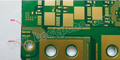
- Use multiple vias under MOSFETs and diodes to reduce thermal resistance.
- Fill vias with thermally conductive epoxy or copper for better heat transfer.
- Place vias in a grid pattern under hot components.
- Via diameter and plating thickness affect thermal performance (larger vias conduct more heat).
3.3. Power Plane and Ground Plane Optimization
- Dedicated Power and Ground Planes:
- Use solid copper planes to distribute heat evenly.
- Avoid splitting planes under high-current paths.
- Multi-Layer Heat Spreading:
- Connect thermal vias to inner copper layers for improved heat dissipation.
- Use thick copper in buried layers to act as a heat sink.
3.4. Component Placement and Layout
- High-Power Components Placement:
- Place MOSFETs, diodes, and inductors away from each other to prevent localized heating.
- Position heat-generating components near the PCB edge or cooling structures.
- Thermal Relief Pads:
- Use thermal relief connections for soldering while ensuring heat dissipation.
- Copper Pour Techniques:
- Add copper fills around hot components to enhance heat spreading.
- Connect copper pours to ground planes for better thermal conduction.
3.5. External Cooling Techniques
- Heat Sinks and Thermal Pads:
- Attach heat sinks to MOSFETs and diodes using thermal interface materials (TIM).
- Use thermally conductive pads for components without direct heat sink mounting.
- Forced Air Cooling:
- Integrate fans or airflow channels in high-power designs.
- Liquid Cooling (for High-Power Applications):
- Embedded microchannels or cold plates for extreme thermal management.
3.6. Simulation and Validation
- Thermal Simulation Tools:
- Use ANSYS Icepak, COMSOL, or Altium’s PDN Analyzer to model heat distribution.
- Infrared Thermography:
- Validate thermal performance using IR cameras in prototype testing.
- Thermal Cycling Tests:
- Ensure reliability under repeated heating/cooling cycles.
4. Case Study: Optimizing a 20A BUCK Converter
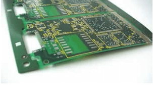
A 20A BUCK converter was designed on a 4-layer PCB with the following improvements:
- Layer Stackup:
- Top Layer: Signal + Power Components (2 oz Cu)
- Inner Layers: Ground & Power Planes (1 oz Cu)
- Bottom Layer: Heat Spreading Copper Pour (2 oz Cu)
- Thermal Vias:
- 0.3mm diameter vias under MOSFETs (filled with copper).
- Cooling:
- Small heat sink on the high-side MOSFET.
- Result:
- Temperature reduced by 15°C compared to a non-optimized design.
5. Conclusion
Effective thermal design in multi-layer PCBs for BUCK converters requires a combination of material selection, copper optimization, thermal vias, strategic component placement, and advanced cooling techniques. By implementing these methods, engineers can achieve better heat dissipation, higher efficiency, and longer operational life in power electronics systems. Future advancements in PCB materials and cooling technologies will further enhance thermal management in high-power BUCK converters.

