Is It Necessary to Remove Dead Copper in PCB Design?
Introduction
Printed Circuit Board (PCB) design involves numerous considerations that affect the performance, reliability, and manufacturability of the final product. One such consideration is the treatment of “dead copper” or “copper islands”—isolated copper areas on the PCB that are not connected to any net or ground plane. The question of whether to remove dead copper has been debated among PCB designers for years, with arguments on both sides. This 2000-word article examines the concept of dead copper, its potential impacts, and whether its removal is truly necessary in modern PCB design.
Understanding Dead Copper
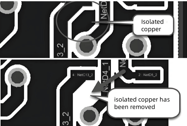
Dead copper refers to isolated copper areas on a PCB layer that have no electrical connection to any other conductive part of the circuit. These areas typically occur when:
- Copper pours are used for ground planes or power distribution
- Automatic copper fill features in PCB design software create continuous copper areas
- Routing decisions leave isolated copper sections between traces
- Board geometries create natural isolation of copper areas
Dead copper can exist on any layer of the PCB, including inner layers in multilayer boards. It’s important to distinguish dead copper from intentional copper features like thermal reliefs or guard rings, which serve specific purposes despite potentially being electrically isolated in certain contexts.
Potential Issues Caused by Dead Copper
1. Manufacturing Concerns
One of the primary reasons designers consider removing dead copper relates to PCB manufacturing:
- Etching Process: During PCB fabrication, the etching process removes unwanted copper. Small, isolated copper areas may not etch away completely or consistently, potentially leading to manufacturing defects.
- Copper Thickness Variation: Large areas of dead copper can affect the uniformity of copper distribution across the board, which might impact plating processes and result in uneven copper thickness.
- Adhesion Problems: Isolated copper features, especially small ones, may have weaker adhesion to the substrate and could potentially peel during manufacturing or assembly processes.
2. Signal Integrity Considerations
Dead copper can influence signal performance in several ways:
- Capacitive Coupling: Isolated copper areas near high-speed signals can create unintended capacitive coupling, potentially affecting signal integrity.
- Antenna Effects: While often overstated, particularly small or narrow dead copper features could theoretically act as miniature antennas, potentially radiating or receiving unwanted electromagnetic interference.
- Impedance Variations: In controlled impedance designs, nearby dead copper can slightly alter the effective dielectric constant and thus change impedance characteristics.
3. Thermal Effects
Copper areas affect heat distribution across the PCB:
- Uneven Thermal Distribution: Dead copper can create localized hot or cold spots by either conducting heat away from certain areas or preventing even heat distribution.
- Soldering Issues: During reflow soldering, large areas of dead copper near components can affect the thermal profile, potentially leading to soldering defects.
Arguments for Keeping Dead Copper
Despite the potential issues, there are several reasons why designers might choose to leave dead copper in place:
1. Manufacturing Benefits
- Improved Etching Uniformity: Some manufacturers argue that maintaining more uniform copper distribution across the board actually improves etching consistency.
- Reduced Processing Time: Removing dead copper increases the amount of copper to be etched, potentially extending processing time and cost.
- Board Stability: The presence of copper, even dead copper, can help maintain board flatness and mechanical stability, especially in large boards or those with uneven copper distribution.
2. Potential Electrical Benefits
- Reduced Crosstalk: In some cases, dead copper between traces can actually help reduce crosstalk by providing additional shielding, even without being grounded.
- EMI Reduction: Copper areas can help contain electromagnetic fields, even when not actively connected to a ground plane.
3. Design Efficiency
- Time Savings: Manually removing dead copper can be time-consuming, especially in complex designs.
- Design Flexibility: Leaving copper in place provides more options for last-minute design changes or re-routing without having to rework copper pours.
Modern PCB Manufacturing Capabilities
Advances in PCB manufacturing have reduced many of the traditional concerns about dead copper:
- Improved Etching Processes: Modern etching techniques can handle fine features and isolated copper areas more effectively than older methods.
- Laser Direct Imaging (LDI): This high-precision imaging technology allows for better control over fine features and isolated copper areas.
- Improved Copper Adhesion: Contemporary PCB materials and treatments have largely mitigated concerns about copper peeling.
These advancements mean that many of the historical reasons for removing dead copper are less relevant with modern fabrication houses.
Design Software Considerations
Most professional PCB design software packages offer automated handling of dead copper:
- Automatic Removal: Many tools can automatically detect and remove dead copper based on user-defined parameters.
- Customizable Settings: Designers can typically set thresholds for what constitutes dead copper (size, isolation distance, etc.) and how it should be handled.
- Real-time Analysis: Some advanced packages can analyze potential dead copper issues during the design phase rather than as a post-processing step.
These software capabilities make dead copper management less of a manual burden for designers.
Industry Practices and Standards
Industry practices regarding dead copper vary:
- High-Frequency/RF Designs: Typically more aggressive about removing dead copper due to sensitivity to parasitic effects.
- High-Density Interconnect (HDI): Often removes dead copper to maximize space and minimize potential manufacturing issues.
- Standard Digital/Analog Designs: Frequently leaves dead copper in place unless it causes specific identified issues.
- Power Electronics: Sometimes keeps dead copper for thermal benefits despite electrical isolation.
There are no universal standards mandating dead copper removal—it remains largely a designer/fabricator preference.
Best Practices for Dead Copper Management
Rather than a binary remove/keep decision, consider these balanced approaches:
- Size-Based Approach: Remove small dead copper islands (e.g., below 0.5mm²) while leaving larger areas.
- Layer-Specific Treatment: Be more aggressive about dead copper removal on outer layers than inner layers.
- Application-Specific Decisions: Consider the sensitivity of your particular design to potential dead copper effects.
- Consult Your Fabricator: Discuss their capabilities and preferences regarding dead copper.
- Design Rules: Set up appropriate design rules in your PCB software to automatically handle dead copper according to your preferences.
Conclusion: Is Removal Necessary?
The necessity of removing dead copper depends on multiple factors:
- For most conventional PCB designs with modern manufacturing, complete dead copper removal is typically not necessary. The potential benefits rarely justify the additional design effort.
- In high-frequency, high-precision, or high-reliability applications, more aggressive dead copper management may be justified to eliminate even minor potential issues.
- The decision should balance manufacturing requirements, design effort, and performance needs for each specific project.
Rather than adopting a universal policy, PCB designers should understand the implications of dead copper and make informed decisions based on their specific design requirements, manufacturing capabilities, and performance targets. In many cases, a moderate approach—removing obviously problematic dead copper while leaving benign areas—provides the best balance between design effort and board performance.
As PCB manufacturing continues to advance, the historical concerns about dead copper become less pressing, allowing designers to focus on more critical aspects of board design. However, awareness of the potential issues ensures that dead copper is properly considered when it might genuinely affect board performance or manufacturability.