PCB Layout Impedance Matching: Principles, Challenges, and Solutions
Introduction
In modern high-speed digital and high-frequency analog circuits, impedance matching in PCB (Printed Circuit Board) layout has become a critical factor affecting system performance. As signal frequencies continue to increase and edge rates become faster, proper impedance control throughout the signal path is essential to maintain signal integrity, minimize reflections, and ensure reliable data transmission.
This article explores the fundamental principles of impedance matching in PCB design, common challenges faced by engineers, and practical solutions to achieve optimal performance. We will examine transmission line theory, various impedance matching techniques, material considerations, and practical layout guidelines to help designers overcome impedance-related issues in their PCB designs.
Understanding Impedance in PCB Layout
Transmission Line Basics
At high frequencies, PCB traces behave not as simple conductors but as transmission lines where the distributed capacitance and inductance along the trace become significant. When the length of a trace approaches about 1/10 of the signal’s wavelength, transmission line effects must be considered.
Characteristic impedance (Z₀) represents the ratio of voltage to current in a transmission line and is determined by:
Z₀ = √(L/C)Where L is the distributed inductance per unit length and C is the distributed capacitance per unit length.
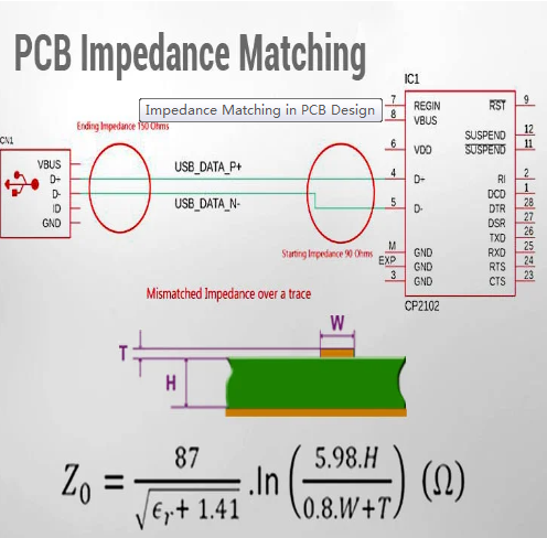
Factors Affecting Trace Impedance
Several geometric and material factors influence a trace’s characteristic impedance:
- Trace width: Wider traces lower impedance (more capacitance)
- Trace thickness: Thicker traces lower impedance
- Dielectric height (H): Greater distance to reference plane increases impedance
- Dielectric constant (εᵣ): Higher εᵣ materials lower impedance
- Solder mask: Affects impedance slightly by changing effective εᵣ
Common Impedance Standards
Various standards define typical impedance values:
- 50Ω: Common for RF systems and single-ended signals
- 75Ω: Used in video applications
- 90-100Ω: Common for differential pairs (USB, Ethernet)
- 100-120Ω: Common for differential signaling (PCIe, DDR)
Impedance Matching Challenges in PCB Design
Signal Reflection Problems
When impedance mismatches occur at any point along the signal path, portion of the signal energy reflects back toward the source. These reflections cause several problems:
- Ringing: Multiple reflections create oscillatory noise
- Signal distortion: Alters signal shape and timing
- Reduced signal amplitude: Decreases signal-to-noise ratio
- EMI radiation: Reflections can radiate electromagnetic interference
The reflection coefficient (Γ) quantifies this mismatch:
Γ = (Z_L - Z₀)/(Z_L + Z₀)Where Z_L is the load impedance and Z₀ is the characteristic impedance.
Common Mismatch Scenarios
- Driver/receiver IC impedance differences: Many ICs have output impedances different from PCB traces
- Connector transitions: Connectors often introduce impedance discontinuities
- Layer changes: Vias between layers create impedance variations
- Trace width changes: Any change in geometry alters impedance
- Branching points: T-junctions or stubs create impedance discontinuities
High-Speed Digital Challenges
Modern high-speed interfaces (DDR memory, PCIe, USB 3.x, etc.) present particular challenges:
- Rise times < 100ps: Make even small discontinuities significant
- Differential pairs: Require careful control of both differential and common-mode impedance
- Skew management: Length matching affects impedance consistency
- Cross-talk: Nearby signals can affect effective impedance
Impedance Matching Techniques
Source-Series Termination
For point-to-point connections, adding a series resistor at the source can match impedances:
R_series = Z₀ - R_driverWhere R_driver is the output impedance of the driving IC.
Advantages:
- Simple implementation
- Reduces power consumption compared to parallel termination
- Minimizes reflections at receiver end
Disadvantages:
- Round-trip delay must be considered for very long traces
- Not suitable for bidirectional buses
Parallel Termination
Placing a resistor equal to Z₀ at the far end of the transmission line:
- Perfectly absorbs incident waves
- Best for very short rise times
- Draws constant DC current (power consideration)
Variations include:
- Thevenin termination: Two resistors providing both termination and bias
- AC termination: Capacitor in series with resistor blocks DC current
Differential Pair Termination
Differential signaling requires attention to both differential (Z_diff) and common-mode (Z_comm) impedance:
Z_diff = 2*Z₀*(1 - k)
Z_comm = Z₀/2*(1 + k)
Where k is the coupling coefficient between traces.
Common techniques include:
- Parallel termination at receiver
- Pi termination network
- Tapped termination for common-mode control
Via Impedance Control
Vias inherently create impedance discontinuities. Mitigation strategies include:
- Via stitching: Multiple small vias in parallel
- Anti-pads: Enlarged clearance holes in reference planes
- Back-drilling: Removal of unused via stubs
- Via-in-pad: Small, filled vias for minimal disruption
PCB Stackup Design for Impedance Control
Material Selection
PCB material properties significantly affect impedance control:
- Dielectric constant (Dk): Affects propagation velocity and impedance
- FR-4: ~4.3 (frequency dependent)
- Rogers materials: 2.2-10.2 (more stable)
- Loss tangent (Df): Affects signal attenuation
- Consistency: Variations in material properties affect impedance tolerance
Layer Stackup Considerations
A well-designed stackup facilitates impedance control:
- Reference planes: Provide consistent return paths
- Symmetry: Prevents board warpage and maintains consistency
- Layer ordering: High-speed signals between ground planes for best isolation
- Cross-hatching: Avoid in reference planes for high-speed signals
Impedance Calculation Methods
- Closed-form equations: For simple microstrip/stripline
- 2D field solvers: More accurate for complex geometries
- 3D EM simulation: For via transitions and complex structures
Common transmission line structures:
- Microstrip: Trace on outer layer with single reference
- Stripline: Trace embedded between two references
- Coplanar waveguide: With ground on same layer
- Differential pairs: Edge-coupled or broadside-coupled
Practical Layout Guidelines
Routing Techniques
- Maintain constant width: Avoid impedance discontinuities
- Minimize bends: Use 45° or curved traces when necessary
- Avoid stubs: Remove unused branches or connector pins
- Length matching: For differential pairs and buses
- Proper spacing: To control cross-talk and maintain impedance
Component Placement
- Termination resistors: Place close to receivers or drivers
- Decoupling capacitors: Proper placement maintains power integrity
- Connectors: Consider impedance transitions at board edges
- High-speed devices: Minimize interconnect lengths
Manufacturing Considerations
- Tolerances: Account for ±10% typical impedance variation
- Etch factor: Traces are trapezoidal, not rectangular
- Solder mask: Affects outer layer impedance slightly
- Surface finish: ENIG, HASL, etc. affect conductor loss
Measurement and Verification
Time Domain Reflectometry (TDR)
TDR instruments:
- Send fast step signal down transmission line
- Measure reflections to locate and quantify impedance discontinuities
- Provide impedance profile along trace length
Vector Network Analysis (VNA)
Measures frequency domain parameters:
- S-parameters (S11 for return loss, S21 for insertion loss)
- Can extract impedance information
- Useful for characterizing materials and interconnects
Simulation Tools
Modern PCB design tools offer:
- Impedance calculators: Built-in or integrated
- Signal integrity analysis: Simulate reflections and eye diagrams
- 3D EM simulation: For complex structures
Advanced Topics
Mixed-Dielectric Environments
Modern PCBs often use:
- Hybrid stackups: Combining FR-4 with high-performance materials
- Embedded components: Affect local impedance
- Flex circuits: Present unique impedance challenges
High-Frequency Considerations
Above 10GHz:
- Material dispersion becomes significant
- Surface roughness affects conductor loss
- Radiation losses increase
Novel Transmission Line Structures
Emerging technologies:
- Broadside-coupled differential pairs
- Offset stripline for lower crosstalk
- Slow-wave structures for size reduction
Conclusion
Proper impedance matching in PCB layout is essential for maintaining signal integrity in modern high-speed designs. By understanding transmission line principles, carefully designing board stackups, implementing appropriate termination strategies, and following good layout practices, designers can overcome impedance matching challenges.
As data rates continue to increase, attention to impedance control becomes even more critical. Future developments in materials, simulation tools, and manufacturing processes will help address the impedance matching challenges of next-generation electronic systems.
Successful PCB design requires balancing electrical requirements with physical constraints, and impedance matching remains at the heart of this balancing act. By applying the principles and techniques discussed in this article, engineers can create PCB layouts that deliver optimal performance while minimizing signal integrity issues related to impedance mismatches.