Automated Soldering Methods for PCB Assembly
Introduction
Printed Circuit Board (PCB) assembly is a critical process in electronics manufacturing, where soldering plays a vital role in establishing electrical connections between components and the board. Traditional manual soldering, while effective for prototyping and small-scale production, is inefficient and inconsistent for high-volume manufacturing. Automated soldering machines have revolutionized PCB assembly by improving precision, speed, and repeatability.
This article explores various automated soldering methods used in PCB manufacturing, including wave soldering, reflow soldering, selective soldering, and laser soldering. Each technique has unique advantages and applications, depending on the PCB design, component types, and production requirements.
1. Wave Soldering
Wave soldering is one of the oldest and most widely used automated soldering techniques for through-hole components. The process involves passing the PCB over a molten solder wave, which forms electrical and mechanical connections between component leads and the board.
Process Steps:
- Flux Application – A flux is applied to remove oxides and improve solder wettability.
- Preheating – The PCB is heated to minimize thermal shock and activate the flux.
- Soldering – The board moves over a wave of molten solder, which adheres to exposed metal surfaces.
- Cooling – The solder solidifies, forming reliable joints.
Advantages:
- High throughput for through-hole components.
- Consistent solder joint quality.
- Suitable for large-scale production.
Limitations:
- Not suitable for surface-mount devices (SMDs).
- Potential for solder bridging or excess solder.
2. Reflow Soldering
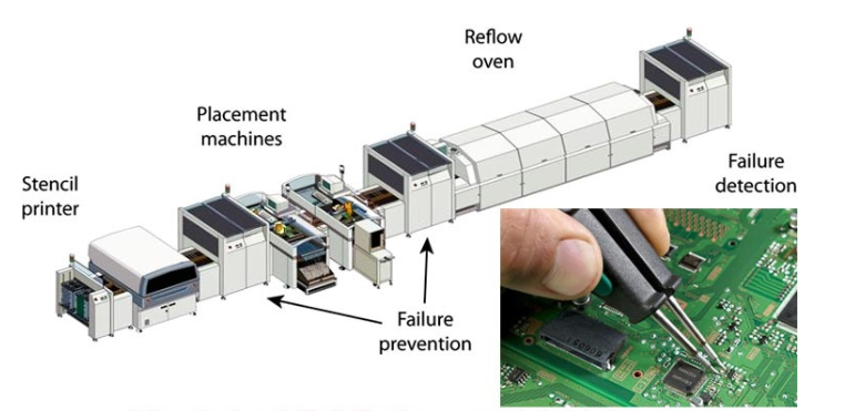
Reflow soldering is the dominant method for assembling surface-mount components. This process involves applying solder paste (a mixture of solder particles and flux) onto PCB pads, placing components, and then heating the assembly in a reflow oven to melt the solder.
Process Steps:
- Solder Paste Application – A stencil printer deposits solder paste onto PCB pads.
- Component Placement – A pick-and-place machine positions SMDs onto the solder paste.
- Reflow Heating – The PCB passes through a multi-zone oven with controlled temperature profiles:
- Preheat (activates flux and removes solvents).
- Soak (equalizes temperature).
- Reflow (melts solder to form joints).
- Cooling (solidifies solder).
Advantages:
- Ideal for high-density SMD assemblies.
- Precise control over solder joint formation.
- Minimal solder waste compared to wave soldering.
Limitations:
- Requires precise temperature profiling.
- Not suitable for through-hole components unless combined with other methods.
3. Selective Soldering
Selective soldering is used when a PCB contains a mix of through-hole and surface-mount components. Unlike wave soldering, which covers the entire board, selective soldering targets specific areas, preventing damage to heat-sensitive components.
Process Steps:
- Flux Application – Spray or droplet flux is applied only to targeted areas.
- Preheating – Localized heating prepares the board for soldering.
- Solder Application – A miniature solder wave or nozzle deposits solder onto selected joints.
Advantages:
- Reduces thermal stress on sensitive components.
- Enables mixed-technology PCB assembly.
- Minimizes solder consumption.
Limitations:
- Slower than wave soldering for high-volume production.
- Requires precise programming for solder nozzle positioning.
4. Laser Soldering
Laser soldering is a high-precision method that uses a focused laser beam to melt solder at specific joints. This technique is ideal for applications requiring minimal heat exposure, such as fine-pitch components and flexible PCBs.
Process Steps:
- Solder Pre-placement – Solder paste or preforms are applied to joints.
- Laser Heating – A controlled laser beam melts the solder without affecting nearby components.
- Cooling – The solder solidifies rapidly, forming a strong connection.
Advantages:
- Extremely precise, suitable for microelectronics.
- Minimal thermal impact on surrounding components.
- No physical contact, reducing contamination risks.
Limitations:
- High equipment cost.
- Slower than other mass soldering methods.
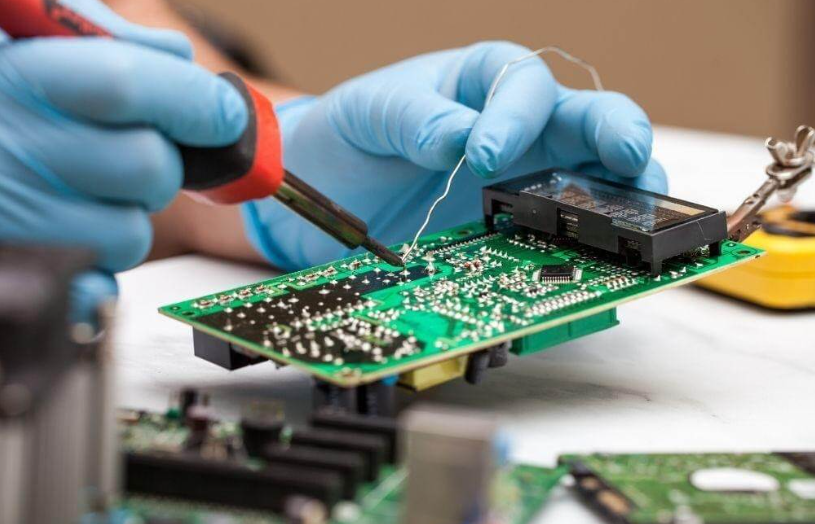
5. Robotic Soldering
Robotic soldering employs programmable robotic arms equipped with soldering irons or dispensers to automate manual soldering tasks. This method is useful for complex or irregular PCB designs that cannot be processed using standard wave or reflow techniques.
Process Steps:
- PCB Positioning – The board is secured in a fixture.
- Soldering Execution – The robot follows programmed paths to apply solder.
- Inspection – Automated optical inspection (AOI) verifies joint quality.
Advantages:
- Flexible for custom or low-volume production.
- Can handle odd-form components.
- Reduces human error in manual soldering.
Limitations:
- Slower than wave or reflow for large batches.
- Requires precise programming and calibration.
Conclusion
Automated soldering methods have significantly enhanced PCB manufacturing by improving efficiency, consistency, and quality. Wave soldering remains ideal for through-hole components, while reflow soldering dominates SMD assembly. Selective soldering bridges the gap for mixed-technology boards, and laser soldering offers unmatched precision for delicate applications. Robotic soldering provides flexibility for specialized assembly needs.
As PCB technology evolves with higher component densities and advanced materials, soldering automation will continue to advance, incorporating AI-driven process optimization and real-time quality control. Manufacturers must select the appropriate soldering method based on production volume, component types, and reliability requirements to achieve optimal results.
By leveraging these automated soldering techniques, electronics manufacturers can ensure high-quality PCB assemblies while reducing costs and production time.