How to Use PCB Manufacturing Files in the Manufacturing and Assembly Process
Introduction
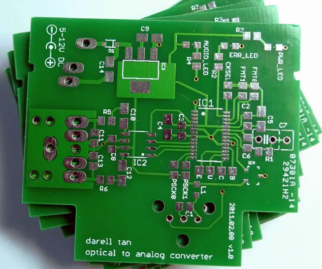
Printed Circuit Boards (PCBs) are essential components in modern electronics, serving as the foundation for mounting and interconnecting electronic components. The PCB manufacturing and assembly process relies heavily on accurate and well-structured manufacturing files to ensure quality, functionality, and efficiency.
This article explores how PCB manufacturing files are used throughout the fabrication and assembly process, detailing their importance, common file formats, and best practices for generating and handling these files.
1. Understanding PCB Manufacturing Files
PCB manufacturing files are digital documents that contain all the necessary information for fabricating and assembling a PCB. These files are generated from PCB design software (such as Altium Designer, KiCad, or Eagle) and are shared with manufacturers to guide production.
Key PCB Manufacturing Files
The most critical files used in PCB manufacturing and assembly include:
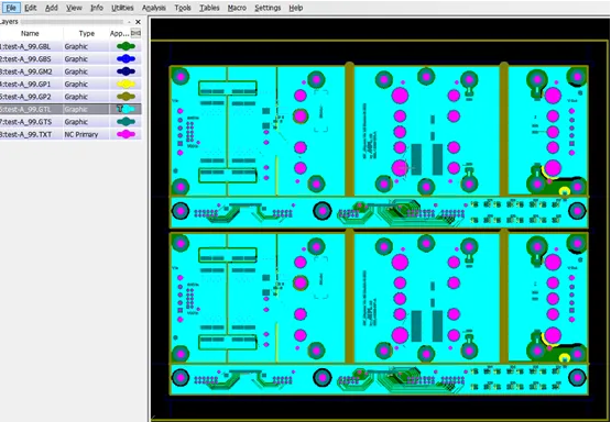
- Gerber Files – The industry-standard format for PCB fabrication, containing layer-by-layer information (copper traces, solder mask, silkscreen, etc.).
- Drill Files (Excellon) – Define the locations and sizes of holes for through-hole components and vias.
- Pick-and-Place Files – Provide coordinates and orientations for surface-mount components during assembly.
- Bill of Materials (BOM) – Lists all components required for assembly, including part numbers, quantities, and reference designators.
- Assembly Drawings – Visual guides showing component placement and orientation.
- Netlist Files – Define electrical connections for verification.
- IPC-356/Netlist Files – Used for testing and validating PCB connectivity.
Each of these files plays a crucial role in different stages of PCB production.
2. PCB Fabrication: Using Gerber and Drill Files
2.1 Gerber Files in PCB Fabrication
Gerber files (RS-274X format) are the most widely used format for PCB fabrication. They describe each layer of the PCB, including:
- Copper layers (signal and power planes)
- Solder mask layers (protective coating over copper)
- Silkscreen layers (component labels and markings)
- Drill drawings (hole locations)
Manufacturers import these files into Computer-Aided Manufacturing (CAM) software to prepare for production. The CAM software checks for errors (e.g., trace spacing, missing layers) before generating toolpaths for PCB milling, etching, and drilling.
2.2 Drill Files (Excellon Format)
Drill files (typically in Excellon format) specify:
- Hole sizes (for vias, through-hole components)
- Drill coordinates (X/Y positions)
- Plating requirements (plated vs. non-plated holes)
The manufacturer uses these files to program drilling machines, ensuring precise hole placement before copper plating (for vias) or component insertion (for through-hole parts).
3. PCB Assembly: Using BOM, Pick-and-Place, and Assembly Drawings
After fabrication, the PCB moves to the assembly phase, where components are soldered onto the board. The following files are critical for this stage:
3.1 Bill of Materials (BOM)
The BOM is a comprehensive list of all components needed for assembly, including:
- Reference designators (e.g., R1, C2, U3)
- Part numbers (manufacturer or distributor codes)
- Descriptions (resistor, capacitor, IC, etc.)
- Quantities (how many of each component are needed)
- Footprint/SMT details (package sizes for automated placement)
A well-structured BOM ensures accurate component sourcing and reduces assembly errors.
3.2 Pick-and-Place Files
For automated assembly, pick-and-place (PnP) machines require:
- X/Y coordinates of each component
- Rotation/orientation (0°, 90°, 180°, etc.)
- Component type (resistor, IC, etc.)
These files are generated from PCB design software and imported into the assembly machine’s software to automate component placement.
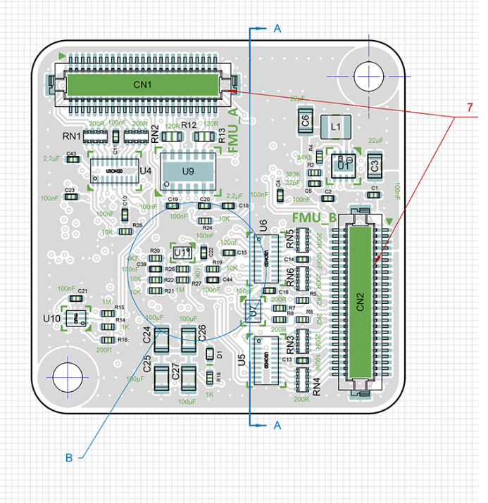
3.3 Assembly Drawings
Assembly drawings provide visual references for:
- Component placement (especially for manual assembly)
- Polarity markings (diodes, capacitors, ICs)
- Special instructions (e.g., “Do not populate” areas)
These drawings help technicians verify correct assembly, especially for prototypes or low-volume production.
4. Testing and Validation: Using Netlists and IPC Files
After assembly, PCBs undergo electrical testing to ensure functionality. Key files used in testing include:
4.1 Netlist Files
Netlist files define electrical connections between components. Testing equipment (such as flying probe or bed-of-nails testers) uses these files to verify:
- Continuity (no open circuits)
- Isolation (no short circuits)
4.2 IPC-356 (Netlist for Bare Board Testing)
IPC-356 files provide additional connectivity data for bare-board testing before assembly. This ensures that the fabricated PCB matches the design before components are added.
5. Best Practices for Generating and Handling PCB Manufacturing Files
To avoid manufacturing delays and defects, follow these best practices:
5.1 File Naming Conventions
Use clear, standardized names (e.g., TopLayer.gbr, DrillFile.txt, BOM_Rev1.csv) to prevent confusion.
5.2 Layer Stack-Up Verification
Ensure Gerber files match the intended PCB layer stack-up (e.g., 2-layer, 4-layer, HDI).
5.3 Design Rule Check (DRC) Before Export
Run DRC in PCB design software to catch errors (e.g., insufficient trace spacing, missing solder mask).
5.4 Include Readme/Notes File
Provide a text file with special instructions (e.g., impedance requirements, unusual materials).
5.5 Verify Files with Gerber Viewers
Before sending files to the manufacturer, inspect them using Gerber viewers (such as Gerbv or online tools) to confirm accuracy.
6. Conclusion
PCB manufacturing files are the backbone of the fabrication and assembly process. Properly generated and managed files ensure high-quality, functional PCBs with minimal errors. By understanding the role of Gerber files, drill files, BOMs, pick-and-place data, and testing files, engineers and manufacturers can streamline production and reduce costly mistakes.
Following best practices in file generation and validation further enhances efficiency, ensuring that the final PCB meets design specifications and performs reliably in its intended application.