Challenges Facing the PCB Design Industry: A Comprehensive Analysis
Introduction
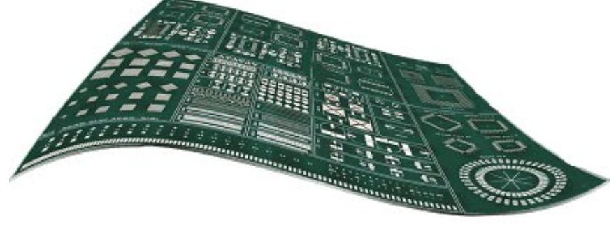
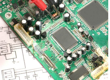
The printed circuit board (PCB) design industry stands at a critical juncture in the electronics manufacturing ecosystem. As the fundamental building block of virtually all modern electronic devices, PCBs have seen exponential growth in demand over the past decades. However, this growth comes with significant challenges that threaten to disrupt the industry’s stability and future development. This 2000-word article examines the multifaceted(difficulties) confronting PCB design professionals and companies today, ranging from technological hurdles to economic pressures and environmental concerns.
1. Technological Challenges in PCB Design
1.1 Increasing Complexity of Electronic Devices
Modern electronics demand PCBs that can accommodate:
- Higher component densities
- Mixed-signal designs (combining analog, digital, and RF circuits)
- Advanced packaging technologies (SiP, SoC, 3D-IC integration)
- High-speed digital interfaces (PCIe 5.0, DDR5, USB4)
This complexity requires designers to master:
- Sophisticated EDA (Electronic Design Automation) tools
- Signal integrity analysis
- Power integrity considerations
- Electromagnetic compatibility (EMC) design techniques
1.2 Miniaturization Pressures
The relentless push for smaller devices creates numerous design challenges:
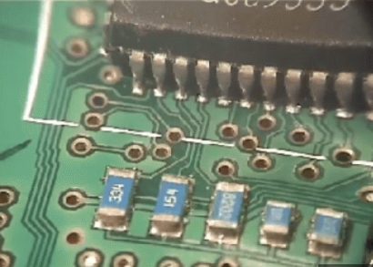
- Fine-pitch components (01005, 0201 packages)
- High-density interconnect (HDI) technologies
- Microvia and blind/buried via structures
- Board thickness reduction while maintaining reliability
1.3 High-Speed Design Demands
With signal speeds exceeding 100Gbps in some applications, designers face:
- Complex impedance control requirements
- Advanced materials with stable dielectric constants
- Crosstalk minimization strategies
- Careful management of signal return paths
1.4 Thermal Management Issues
Increased power densities lead to:
- Hotspot formation
- Thermal expansion mismatches
- Reliability concerns from repeated thermal cycling
- Challenges in heat dissipation for sealed devices
2. Workforce and Skills Gap
2.1 Aging Workforce and Knowledge Transfer
The industry faces:
- Retiring experienced designers taking decades of knowledge
- Inadequate training programs for new designers
- Lengthy learning curves for complex design tools
- Shortage of mentors for junior designers
2.2 Multidisciplinary Knowledge Requirements
Modern PCB designers need expertise in:
- Electrical engineering fundamentals
- Materials science
- Mechanical design considerations
- Manufacturing processes
- Thermal dynamics
- Software tools and scripting
2.3 Training and Education Shortcomings
Educational institutions struggle with:
- Outdated curricula not matching industry needs
- Limited access to advanced EDA tools
- Lack of practical manufacturing knowledge
- Insufficient emphasis on high-speed design principles
3. Economic and Market Pressures
3.1 Cost Reduction Demands
OEMs constantly pressure PCB designers to:
- Reduce layer counts
- Use cheaper materials
- Minimize board sizes
- Accept longer design cycles
3.2 Shortened Product Life Cycles
The rapid pace of technological change leads to:
- Shorter design windows
- More frequent redesigns
- Increased revision cycles
- Pressure for first-time-right designs
3.3 Supply Chain Disruptions
Recent global events have highlighted vulnerabilities:
- Component shortages forcing redesigns
- Long lead times for advanced materials
- Geopolitical factors affecting material availability
- Price volatility in copper and other raw materials
3.4 Outsourcing and Offshoring Pressures
Many companies face:
- Competition from low-cost design centers
- Loss of institutional knowledge
- Quality control challenges with offshore partners
- Intellectual property protection concerns
4. Environmental and Regulatory Challenges
4.1 RoHS and REACH Compliance
Designers must navigate:
- Lead-free soldering requirements
- Restricted substance lists
- Material documentation requirements
- Testing and certification processes
4.2 Waste Electrical and Electronic Equipment (WEEE) Directives
These regulations impact design through:
- Requirements for recyclability
- Disassembly considerations
- Material selection constraints
- End-of-life processing requirements
4.3 Conflict Minerals Regulations
Designers must ensure their supply chains avoid:
- Tin, tantalum, tungsten, and gold from conflict regions
- Unethical mining practices
- Non-compliant suppliers
4.4 Sustainable Design Pressures
Growing environmental awareness drives:
- Demand for biodegradable substrates
- Reduced energy consumption requirements
- Longer product lifespans
- Repair-friendly designs
5. Tools and Design Process Challenges
5.1 EDA Tool Limitations
Designers frequently encounter:
- High software licensing costs
- Steep learning curves
- Inadequate tool integration
- Limited automation capabilities
- Incomplete design rule checks
5.2 Design-Manufacturing Handoff Issues
Common problems include:
- Incomplete or ambiguous design documentation
- Manufacturing capabilities not considered during design
- Poor communication between design and fabrication teams
- Lack of standardized data exchange formats
5.3 Version Control and Collaboration Difficulties
Distributed design teams face:
- File management challenges
- Revision control problems
- Simultaneous editing conflicts
- Lack of real-time collaboration tools
5.4 Design Reuse Barriers
Obstacles to effective IP reuse include:
- Poor documentation of existing designs
- Lack of standardization
- Context-specific optimizations
- Changing component availability
6. Emerging Technology Disruptions
6.1 Flexible and Stretchable Electronics
These new technologies require:
- Completely different design methodologies
- New material understanding
- Novel reliability testing approaches
- Different manufacturing processes
6.2 Additive Manufacturing of Electronics
3D printing technologies bring:
- Uncertainty about design rules
- Unproven reliability data
- Limited material options
- New design freedom requiring new thinking
6.3 Embedded Components
Integration of passive and active components within the board presents:
- Thermal management challenges
- Testing difficulties
- Repair limitations
- Design rule complexities
6.4 Photonic Integrated Circuits
The emerging field of optical PCBs requires:
- New skill sets
- Different material properties understanding
- Alternative signal integrity approaches
- Hybrid electronic-photonic design techniques
7. Intellectual Property and Security Concerns
7.1 Design Theft Risks
Increasing concerns about:
- Unauthorized copying of board designs
- Reverse engineering vulnerabilities
- Supply chain security
- Counterfeit components
7.2 Cybersecurity Threats
PCB designers must consider:
- Hardware attack surfaces
- Side-channel vulnerabilities
- Firmware protection
- Secure boot implementations
7.3 Export Control Regulations
Designs containing advanced technologies face:
- International traffic in arms regulations (ITAR)
- Export administration regulations (EAR)
- Country-specific restrictions
- Compliance documentation burdens
Conclusion: Navigating the Challenges
The PCB design industry faces a perfect storm of technological, economic, and regulatory challenges that threaten to disrupt traditional ways of working. However, these困境 (difficulties) also present opportunities for innovation and improvement. Successful navigation of these challenges will require:
- Investment in Education and Training – Developing comprehensive programs to train the next generation of designers and upskill current professionals.
- Tool Development and Automation – Creating more intelligent EDA tools that can handle increasing complexity while reducing designer workload.
- Collaborative Ecosystems – Building stronger connections between designers, manufacturers, and suppliers to improve design for manufacturability.
- Standardization Efforts – Developing industry-wide standards for design reuse, data exchange, and manufacturing handoff.
- Sustainable Practices – Embracing environmentally conscious design approaches that meet regulatory requirements while maintaining performance.
- Security Integration – Incorporating security considerations at the fundamental design level rather than as an afterthought.
The PCB design industry has consistently demonstrated remarkable adaptability throughout its history. By addressing these challenges head-on, the industry can continue to serve as the foundation for electronic innovation in the decades to come. Those companies and professionals who proactively tackle these issues will position themselves as leaders in the next era of electronic design.