The Consequences of Copper-less Vias in PCBs: Causes, Effects, and Solutions
Introduction
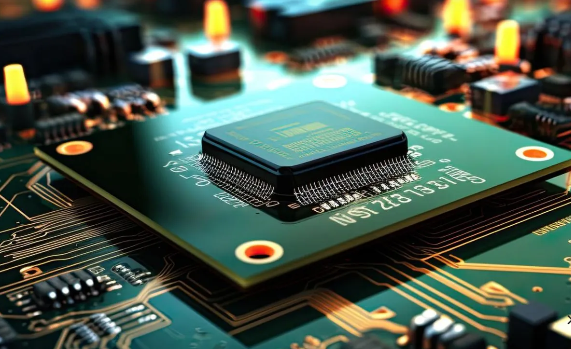
Printed Circuit Boards (PCBs) are essential components in modern electronics, providing mechanical support and electrical connections between components. Vias—small holes drilled into PCBs—play a critical role in establishing electrical connectivity between different layers of a multi-layer board. These vias are typically plated with copper to ensure conductivity. However, when a via lacks copper plating (a condition known as a “copper-less via” or “non-plated via”), it can lead to significant functional and reliability issues.
This article explores the causes, effects, and potential solutions for copper-less vias in PCBs, providing insights for designers, manufacturers, and quality control professionals.
1. What Causes Copper-less Vias in PCBs?
Several factors can lead to incomplete or absent copper plating in PCB vias:
1.1. Poor Plating Process
The electroplating process deposits copper onto the walls of drilled holes. If the plating bath has insufficient copper concentration, improper current density, or contamination, the via may not be fully plated.
1.2. Inadequate Hole Cleaning
Before plating, drilled holes must be cleaned to remove debris and ensure proper adhesion. Residual drilling dust or contaminants can prevent copper from bonding correctly, leading to voids or weak plating.
1.3. Drilling Damage
If the drilling process generates excessive heat or mechanical stress, it can smear resin over the hole walls, making copper deposition difficult.
1.4. Insufficient Electroless Copper Deposition
Before electroplating, a thin layer of electroless copper is applied to facilitate conductivity. If this step fails, subsequent electroplating will be ineffective.
1.5. Over-Etching During PCB Fabrication
Excessive etching can remove too much copper, thinning or completely eliminating the via’s conductive layer.
1.6. Thermal Stress and Microcracks
Repeated thermal cycling (e.g., during soldering) can cause microcracks in the copper plating, eventually leading to open circuits.
2. What Happens When a PCB Via Has No Copper?
A copper-less via disrupts the intended electrical pathway, leading to various problems:
2.1. Open Circuits
The primary issue is an open circuit, where signals cannot pass between layers. This can cause:
- Complete device failure if critical power or ground connections are lost.
- Intermittent faults if the connection degrades over time.
2.2. Increased Resistance and Signal Integrity Issues
Even partially plated vias introduce higher resistance, leading to:
- Signal attenuation in high-frequency circuits.
- Voltage drops in power delivery networks.
- Cross-talk and EMI problems due to impedance mismatches.
2.3. Poor Thermal Conductivity
Copper-plated vias help dissipate heat. Without copper:
- Components may overheat, reducing lifespan.
- Thermal stress increases, leading to delamination or warping.
2.4. Mechanical Weakness
Copper plating reinforces via structures. Unplated vias are more prone to:
- Cracking during assembly or operation.
- Delamination under thermal or mechanical stress.
2.5. Manufacturing and Rework Challenges
- Difficult troubleshooting: Open vias are hard to detect without advanced testing.
- Costly rework: Repairing defective vias often requires drilling and manually filling them.
3. How to Detect Copper-less Vias?
Early detection prevents field failures. Common inspection methods include:
3.1. Automated Optical Inspection (AOI)
- Checks for visible defects but may miss internal plating issues.
3.2. Microsectioning (Cross-Section Analysis)
- Destructive testing that reveals plating thickness and voids.
3.3. Electrical Testing (Flying Probe, ICT)
- Verifies continuity and resistance.
3.4. X-ray Inspection
- Non-destructive method to examine internal via structures.
3.5. Thermal Imaging
- Detects hotspots caused by poor thermal conduction.
4. How to Prevent and Fix Copper-less Vias?
4.1. Prevention Strategies
- Optimize plating parameters: Ensure proper current density and bath chemistry.
- Improve hole cleaning: Use plasma or chemical desmearing.
- Use high-quality drill bits: Minimize resin smear.
- Implement process controls: Monitor plating thickness with real-time sensors.
4.2. Repair Techniques
- Conductive epoxy filling: Manually fills defective vias.
- Via-in-pad rework: Re-drill and replate affected areas.
- Wire jumpers: Bypass open vias with external wiring (not ideal for high-speed designs).
5. Conclusion
Copper-less vias in PCBs can lead to catastrophic failures, signal degradation, and reduced product lifespan. Understanding the root causes—such as plating defects, drilling issues, and thermal stress—helps in implementing preventive measures. Advanced inspection techniques like X-ray and cross-sectioning are essential for early detection, while proper manufacturing controls minimize risks.
For high-reliability applications, designers should consider alternative via structures (e.g., filled vias, tented vias) and rigorous testing protocols to ensure robust PCB performance.
By addressing copper-less vias proactively, manufacturers can enhance yield, reduce rework costs, and deliver more reliable electronic products.