Methods for PCB Reverse Engineering: A Comprehensive Guide
Introduction
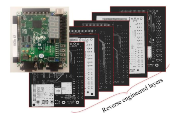
Printed Circuit Board (PCB) reverse engineering, often referred to as PCB “剖制” in Chinese technical terminology, is the process of analyzing and reconstructing the design of an existing PCB. This practice serves numerous legitimate purposes including legacy system maintenance, competitive analysis (where legal), repair of equipment with unavailable documentation, and educational research. As technology continues to advance, the methods for PCB reverse engineering have evolved significantly. This 2000-word article explores the various techniques available for PCB reverse engineering, their applications, advantages, and limitations.
Section 1: Non-Destructive Analysis Methods
1.1 Visual Inspection and Photography
The most fundamental approach to PCB reverse engineering begins with thorough visual examination:
- Macro Photography: High-resolution cameras capture board details at various angles
- Microscopy: Stereo microscopes (typically 10x-50x magnification) reveal fine traces and components
- Multispectral Imaging: Different light wavelengths (UV, IR) can highlight various board features
- Measurement Tools: Calipers and micrometers document physical dimensions
Advantages: Non-invasive, preserves original board, low cost
Limitations: Cannot reveal internal layers, limited by component density
1.2 X-Ray Imaging
For multilayer boards or obscured components:
- 2D X-Ray: Provides planar views showing internal layer relationships
- 3D X-Ray Tomography: Computed tomography reconstructs volumetric models
- Automated X-Ray Inspection (AXI): Systems like Nordson DAGE combine automation with analysis
Applications: BGA package inspection, via analysis, layer counting
Equipment Cost: $50,000-$500,000 for industrial systems
1.3 Infrared Thermography
- Identifies active components during operation
- Maps thermal signatures to functional blocks
- Helps understand power distribution networks
Section 2: Destructive Layer-by-Layer Analysis
2.1 Mechanical Delamination
Traditional approach for multilayer boards:
- Milling: Precision CNC mills remove layers sequentially
- Polishing: Cross-section preparation for microscopic analysis
- Layer Imaging: Each exposed layer photographed and documented
Challenges: Risk of damaging fragile traces, time-consuming
2.2 Chemical Etching
Alternative to mechanical methods:
- Ferric Chloride Etching: Dissolves copper while preserving substrate
- Acidic Solutions: For specific metal compositions
- Plasma Etching: More controlled removal in vacuum chambers
Safety Considerations: Requires proper ventilation and disposal procedures
2.3 Laser Ablation
Emerging high-precision technique:
- UV Lasers: Remove material with micron-level precision
- Layer-by-Layer Removal: Software-controlled process
- In-situ Imaging: Integrated cameras document each layer
Systems Cost: $100,000-$1M for industrial laser reverse engineering stations
Section 3: Electrical Analysis Techniques
3.1 Continuity Testing
Basic but essential method:
- Multimeter Testing: Verifies connections between points
- Network Analysis: Maps electrical relationships
- Signature Analysis: Compares with known good boards
3.2 Boundary Scan (JTAG)
For compatible digital circuits:
- IEEE 1149.1 Standard: Accesses test access ports (TAPs)
- Register Analysis: Maps device interconnections
- BSD Files: Boundary Scan Description files aid interpretation
3.3 Signal Probing and Analysis
Active circuit examination:
- Logic Analyzers: Capture digital signal relationships
- Oscilloscopes: Analog signal characteristics
- Non-contact Probes: Magnetic current probes, E-field sensors
Section 4: Software-Assisted Reconstruction
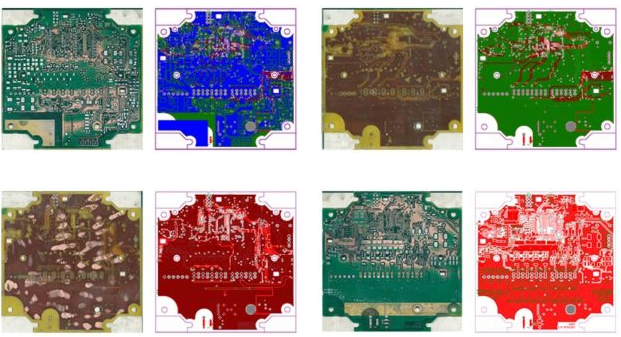
4.1 Image Processing Algorithms
Automating visual reconstruction:
- Trace Recognition: Converts board images to vector formats
- Component Recognition: Machine learning identifies parts
- Layer Alignment: Aligns images from different layers
4.2 Schematic Reconstruction Tools
Specialized software solutions:
- PCB Reverse Engineering Suites: Dedicated packages like OpenRE, PCBRL
- EDA Software Plugins: Extensions for Altium, KiCad, etc.
- Custom Scripts: Python/OpenCV-based automation
4.3 3D Reconstruction
Creating comprehensive models:
- CT Scan Reconstruction: From X-ray tomography data
- Photogrammetry: From multiple angle photographs
- Hybrid Approaches: Combining multiple data sources
Section 5: Specialized Applications
5.1 High-Density Interconnect (HDI) Boards
Challenges:
- Microvias and buried vias
- Finer trace geometries (<50μm)
- Advanced materials (flex, ceramic)
Solutions:
- Higher resolution imaging
- Advanced laser ablation
- Nano-CT scanning
5.2 RF and Microwave PCBs
Considerations:
- Transmission line analysis
- Material dielectric characterization
- Impedance matching reconstruction
5.3 Flexible and Rigid-Flex PCBs
Special Techniques:
- Layer separation without damage
- Stress pattern analysis
- Flexible substrate handling
Section 6: Legal and Ethical Considerations
Important factors before reverse engineering:
- Patent Infringement: Some designs are legally protected
- Copyright Issues: PCB layouts may have copyright protection
- Trade Secrets: Varies by jurisdiction
- DMCA: Digital Millennium Copyright Act implications (U.S.)
- Clean Room Design: Legal approach to avoid infringement
Best Practice: Always consult legal experts before commercial applications
Section 7: Emerging Technologies
Future directions in PCB reverse engineering:
- AI-Assisted Analysis: Machine learning for automated recognition
- Quantum Sensing: For non-invasive internal imaging
- Atomic Force Microscopy: For nanometer-scale analysis
- Terahertz Imaging: Penetrating non-conductive materials
Conclusion
PCB reverse engineering encompasses a diverse array of methods ranging from simple visual inspection to advanced computational imaging techniques. The optimal approach depends on multiple factors including:
- Board complexity (layer count, density)
- Available equipment and budget
- Time constraints
- Required accuracy
- Preservation requirements
As electronic devices continue to proliferate across industries, the importance of PCB reverse engineering skills will only grow. However, practitioners must balance technical capabilities with legal and ethical responsibilities. The field continues to evolve with new imaging technologies, smarter software tools, and more sophisticated analysis methods pushing the boundaries of what’s possible in PCB reconstruction.
For those entering this field, developing a systematic methodology that combines multiple complementary techniques typically yields the best results. Starting with non-destructive methods before proceeding to more invasive techniques preserves options and information throughout the analysis process. Documentation at each stage is critical, as is maintaining strict version control of all reconstructed files and images.
The future of PCB reverse engineering lies in the integration of automated systems with human expertise—leveraging machine learning for pattern recognition while applying engineering knowledge to interpret results and validate reconstructions. As this technology advances, it will enable faster, more accurate analysis of increasingly complex electronic systems.