What is PCB Panelization and Why is it Important?
Introduction to PCB Panelization
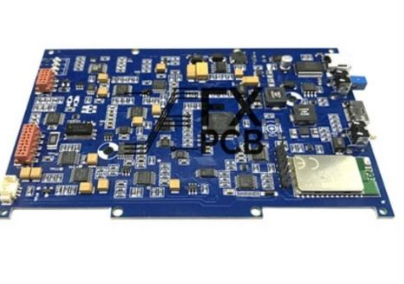
Printed Circuit Board (PCB) panelization is a manufacturing technique where multiple individual PCB designs are grouped together into a single, larger board (called a panel) for production. This approach allows manufacturers to produce several PCBs simultaneously during a single manufacturing run, significantly improving efficiency and reducing costs.
The concept of panelization has become fundamental in modern electronics manufacturing, particularly for small to medium-sized PCBs. By combining multiple boards into one panel, manufacturers can optimize material usage, streamline assembly processes, and maintain consistent quality across all units.
Understanding the PCB Panelization Process
Basic Principles of Panelization
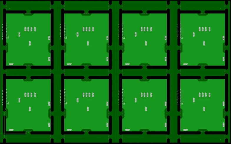
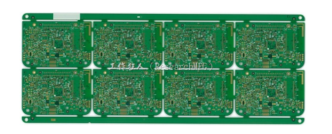
PCB panelization involves arranging multiple PCB designs in a specific configuration on a standard panel size that matches the manufacturer’s equipment capabilities. The most common panel sizes are 18″ × 24″ or 16″ × 18″, though these can vary depending on the fabrication facility.
The individual PCBs within the panel are connected through various methods:
- V-score (V-groove): A partial cut that leaves a thin section of material connecting the boards
- Tab routing: Small tabs of material that hold boards together with perforations for easy separation
- Perforated tabs: Similar to tab routing but with regularly spaced holes along the connection
- Breakaway tabs: Thin connections designed to snap apart cleanly
Design Considerations for Panelization
Effective panelization requires careful planning during the PCB design phase. Key considerations include:
- Board Orientation: Arranging boards to maximize panel space utilization
- Clearance: Maintaining adequate spacing between boards for routing or scoring
- Fiducial Marks: Adding alignment markers for automated assembly equipment
- Tooling Holes: Including holes for panel handling and alignment during manufacturing
- Breakaway Tabs: Positioning tabs that won’t interfere with components or functionality
- Panel Strength: Ensuring the panel remains sturdy throughout the manufacturing process
Why PCB Panelization is Important
Manufacturing Efficiency
Panelization dramatically improves manufacturing efficiency by:
- Reducing handling time (multiple boards processed simultaneously)
- Minimizing setup changes between different board designs
- Optimizing the use of raw materials (less waste between individual boards)
- Enabling batch processing of identical boards
A well-designed panel can increase throughput by 300-500% compared to processing individual boards, making it essential for mass production.
Cost Reduction
The economic benefits of panelization are substantial:
- Material Savings: More efficient use of laminate materials reduces waste
- Labor Savings: Automated equipment can process many boards in a single operation
- Equipment Utilization: Maximizes the use of expensive manufacturing equipment
- Shipping Efficiency: Panels are easier to handle and ship than individual small boards
For high-volume production, panelization can reduce per-unit costs by 20-40%, making it crucial for competitive pricing.
Assembly Process Optimization
Modern surface-mount technology (SMT) assembly lines are designed to work with standardized panel sizes. Panelization enables:
- Automated component placement across multiple boards simultaneously
- Consistent solder paste application for all boards in a panel
- Efficient wave soldering processes for through-hole components
- Simplified handling during conformal coating or other post-assembly processes
Quality Control Benefits
Panelization contributes to consistent quality by:
- Ensuring identical manufacturing conditions for all boards in a panel
- Reducing handling-related defects (boards are manipulated less frequently)
- Facilitating automated optical inspection (AOI) of multiple units in one scan
- Enabling simultaneous testing of multiple boards
Types of PCB Panelization
Standard Panelization
The most common approach where identical PCBs are arranged in a grid pattern. This is used for high-volume production of a single design.
Mixed Panelization (Multi-Circuit Panel)
Combining different PCB designs in one panel. This is particularly useful for:
- Prototyping multiple designs simultaneously
- Manufacturing companion boards that will be used together
- Small production runs where full panels of a single design aren’t justified
Step-and-Repeat Panelization
Creating panels with multiple copies of the same design arranged in a repeating pattern. This is the most efficient method for mass production.
Custom Panelization
Special arrangements designed for unique board shapes or specific manufacturing requirements, often involving creative nesting of irregularly shaped PCBs.
Technical Aspects of PCB Panelization
V-Scoring Techniques
V-scoring creates angled grooves (typically 30-35 degrees) that penetrate about 1/3 of the board thickness from both sides. This method offers:
- Clean break edges after separation
- Minimal material waste
- Space efficiency (boards can be placed closer together)
- Suitability for rectangular boards
Tab Routing Considerations
Tab routing uses small connecting bridges (typically 3-5mm wide) with perforations for easy breakaway. This method is preferred for:
- Irregularly shaped boards
- Designs requiring stronger panel connections
- Boards that might warp during processing
- Situations where clean edges are less critical
Breakaway Tab Design
Effective tab design must balance panel strength with easy separation:
- Tab width typically 0.05-0.1 inches
- Perforations or mouse bites (small drilled holes) along the tab
- Strategic placement to avoid component interference
- Consideration of depaneling method (manual vs. automated)
Depaneling Methods
After assembly, individual PCBs must be separated from the panel. Common methods include:
Manual Breakaway
Suitable for low-volume production or prototypes:
- Simple and low-cost
- Risk of board damage or stress
- Inconsistent results
Punch and Die
Used for high-volume production of standardized designs:
- Fast and precise
- High initial tooling cost
- Limited to specific board shapes
Router Depaneling
Uses a CNC router to cut boards apart:
- Precise cutting
- Suitable for complex shapes
- Generates dust that requires cleanup
Laser Depaneling
Advanced method offering:
- Extremely precise cuts
- No mechanical stress on boards
- High equipment cost
- Fast processing
Challenges and Solutions in PCB Panelization
Common Panelization Challenges
- Board Warping: Uneven stress can cause panels to warp during processing
- Component Clearance: Tall components near panel edges may interfere with manufacturing equipment
- Depaneling Damage: Improper separation can damage boards or components
- Mixed Technology Issues: Combining different board types may create processing conflicts
- Material Waste: Poor panel design can lead to excessive scrap
Best Practices for Effective Panelization
- Early Collaboration: Involve your PCB manufacturer in the panel design process
- Standardization: Use common panel sizes compatible with your manufacturer’s equipment
- Clearance Planning: Allow adequate space for routing, scoring, and depaneling
- Tooling Marks: Include fiducials and tooling holes for precise alignment
- Stress Analysis: Consider thermal and mechanical stresses during assembly
- Depaneling Method: Design your panel for the intended separation method
- Quality Verification: Build test panels to validate your design before full production
The Future of PCB Panelization
Emerging Trends
- Smart Panelization Software: Advanced algorithms that automatically optimize panel layouts
- Flexible Panel Designs: Accommodating more complex and irregular board shapes
- Integrated Testing: Incorporating test circuits directly into panel designs
- Sustainable Practices: Reducing material waste through innovative panel layouts
- Hybrid Materials: Panels combining different substrate materials for specialized applications
Industry 4.0 Integration
Modern panelization is increasingly connected with:
- Digital twin technology for virtual prototyping
- AI-driven design optimization
- Automated quality control systems
- IoT-enabled manufacturing tracking
Conclusion: The Critical Role of PCB Panelization
PCB panelization is far more than just a manufacturing convenience—it’s a fundamental aspect of efficient, cost-effective electronics production. By enabling simultaneous processing of multiple boards, panelization delivers substantial benefits in terms of:
- Reduced production costs
- Improved manufacturing efficiency
- Enhanced quality control
- Optimized material usage
- Streamlined assembly processes
As PCB technology continues to advance with smaller components, higher densities, and more complex designs, the importance of proper panelization only grows. Whether you’re producing simple consumer devices or sophisticated aerospace electronics, understanding and implementing effective panelization techniques can mean the difference between a profitable product and a manufacturing headache.
For PCB designers and manufacturers alike, investing time in proper panelization planning pays dividends throughout the product lifecycle—from prototype to mass production. In today’s competitive electronics market, panelization isn’t just important—it’s essential.