How to Prevent PCB Reverse Engineering and Cloning in PCB Design
Introduction
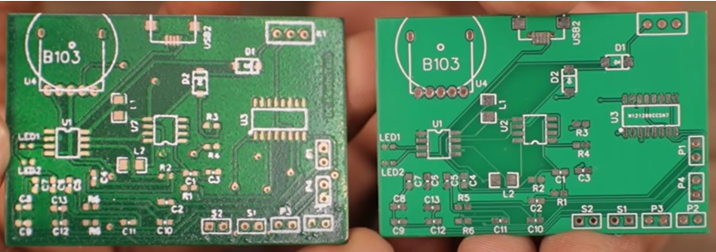
Printed Circuit Board (PCB) design is a critical aspect of modern electronics, encompassing everything from consumer gadgets to industrial machinery. However, with the increasing sophistication of reverse engineering techniques, protecting PCB designs from cloning and unauthorized duplication has become a significant concern for manufacturers and designers.
Reverse engineering a PCB involves analyzing its layout, components, and connections to replicate or modify the design without permission. This can lead to intellectual property theft, counterfeit products, and financial losses. To combat this, PCB designers must implement various strategies to make reverse engineering more difficult, time-consuming, or even impossible.
This article explores several effective methods to prevent PCB cloning, including obfuscation techniques, security measures, and legal protections.
1. Obfuscation Techniques to Hide Circuit Functionality
One of the simplest ways to deter reverse engineering is to make the PCB design difficult to understand. Obfuscation techniques involve modifying the board layout to confuse potential copiers.
A. Using Multi-Layer PCBs with Buried and Blind Vias
- A multi-layer PCB (4+ layers) is harder to reverse-engineer than a single or double-layer board.
- Blind vias (connecting outer layers to inner layers) and buried vias (connecting inner layers only) make tracing connections difficult.
- Attackers must delaminate the PCB to analyze internal traces, which is destructive and time-consuming.
B. Unconventional Routing and Dummy Traces
- Route signals in non-intuitive ways, such as serpentine patterns or looping traces.
- Add dummy traces (non-functional connections) to mislead reverse engineers.
- Use false ground/power planes that appear functional but serve no real purpose.
C. Component Masking and Silkscreen Tricks
- Remove or obscure component markings (e.g., sanding off IC labels).
- Use identical-looking components with different functions (e.g., resistors in place of capacitors).
- Place misleading silkscreen labels to confuse attackers.
2. Secure PCB Design Practices
Beyond obfuscation, implementing secure design practices can significantly enhance protection against cloning.
A. Encrypted Firmware and Secure Microcontrollers
- Use microcontrollers with read-out protection (e.g., STM32’s RDP levels, ARM TrustZone).
- Encrypt firmware to prevent extraction via debugging interfaces (JTAG, SWD).
- Employ secure boot mechanisms to ensure only authorized code runs.
B. Custom or Proprietary Components
- Design ASICs (Application-Specific Integrated Circuits) or custom FPGAs that are not commercially available.
- Use obsolete or hard-to-source components to make replication difficult.
C. Tamper-Proof and Self-Destructive Features
- Implement tamper detection circuits that erase firmware or disable the board if opened.
- Use epoxy-coated PCBs or potting compounds to prevent physical probing.
- Integrate anti-tamper meshes (conductive traces that trigger alarms if broken).

3. Anti-Cloning Technologies and Countermeasures
Several advanced technologies can be integrated into PCB designs to prevent unauthorized copying.
A. Hardware Authentication Chips
- Use secure authentication ICs (e.g., Maxim’s DS28E15, Microchip’s ATECC608A).
- These chips store cryptographic keys and require challenge-response authentication before allowing system operation.
B. Unique Board Identifiers and Serialization
- Embed unique serial numbers in each PCB (e.g., via laser engraving or programmable EEPROMs).
- Implement blockchain-based tracking to verify authenticity.
C. Active Shield Layers
- Some high-security PCBs use active mesh shielding—a grid of traces that detect tampering by monitoring capacitance/resistance changes.
- If an attacker drills into the board, the circuit detects the intrusion and locks or erases critical data.
4. Legal and Supply Chain Protections
Technical measures alone may not be enough; legal and supply chain strategies are also essential.
A. Patents and Intellectual Property (IP) Protection
- File for patents on unique circuit designs.
- Use non-disclosure agreements (NDAs) with manufacturers.
B. Trusted Manufacturing Partners
- Work only with certified PCB fabrication and assembly houses.
- Avoid sharing complete design files—provide only necessary layers for production.
C. Obfuscated Gerber Files
- Modify Gerber files before sending them to manufacturers by:
- Removing component designators.
- Using generic layer names.
- Splitting critical connections across multiple files.
5. Testing and Validation Against Reverse Engineering
Before finalizing a design, test its resistance to reverse engineering:
- Physical Attack Testing: Attempt to delaminate the PCB or probe traces.
- Firmware Extraction Attempts: Try dumping firmware via debug ports.
- X-ray and Microscope Analysis: Check if internal traces are easily visible.

Conclusion
Preventing PCB reverse engineering requires a multi-layered approach, combining obfuscation techniques, secure design practices, anti-cloning technologies, and legal protections. While no method is 100% foolproof, implementing these strategies significantly increases the difficulty and cost of copying a design, discouraging most attackers.
As reverse engineering tools become more advanced, PCB designers must stay ahead by adopting encrypted firmware, tamper-proofing mechanisms, and authentication protocols. By integrating these security measures early in the design process, companies can better protect their intellectual property and maintain a competitive edge in the electronics industry.
Final Recommendations
✔ Use multi-layer PCBs with blind/buried vias.
✔ Encrypt firmware and secure microcontrollers.
✔ Implement tamper detection and self-destruct mechanisms.
✔ Work with trusted manufacturers and protect design files.
✔ Regularly test designs against reverse engineering attempts.
By following these guidelines, PCB designers can significantly reduce the risk of cloning and ensure their innovations remain secure.