Optimal PCB Layout Design for Mobile Phones: Key Considerations and Best Practices
1. Introduction
The rapid evolution of mobile phone technology demands increasingly complex and compact Printed Circuit Board (PCB) designs. A well-optimized PCB layout is crucial for ensuring signal integrity, power efficiency, thermal management, and electromagnetic compatibility (EMC). This article explores the fundamental principles and best practices for PCB layout design in mobile phones, focusing on component placement, routing strategies, and design for manufacturability (DFM).
2. Key Considerations in Mobile PCB Layout Design
2.1 Component Placement and Stackup Design
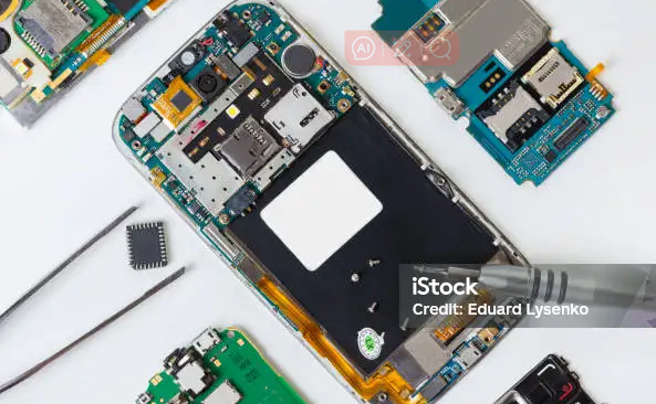
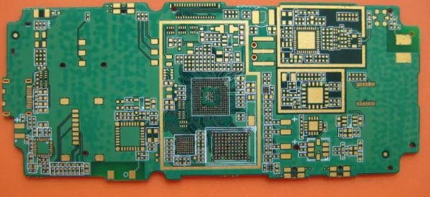
Mobile PCBs are typically high-density interconnect (HDI) boards with multiple layers (6-12 layers or more). Proper stackup design is essential to minimize signal interference and optimize power distribution.
- Critical Component Placement:
- Place high-speed components (e.g., processors, memory, RF modules) close to their power sources to minimize parasitic inductance.
- Position noise-sensitive analog circuits (e.g., audio codecs, sensors) away from digital and RF sections.
- Ensure proper thermal management by placing heat-generating components (e.g., power amplifiers, PMICs) near heat dissipation paths.
- Layer Stackup Strategy:
- Use dedicated power and ground planes to reduce noise and improve signal integrity.
- Route high-speed signals on inner layers between ground planes to minimize crosstalk.
2.2 Signal Integrity and High-Speed Routing
Modern smartphones support high-speed interfaces such as DDR memory, USB 3.0, PCIe, and MIPI. Proper routing techniques are necessary to maintain signal integrity.
- Impedance Control:
- Match trace widths and dielectric spacing to maintain consistent impedance (e.g., 50Ω for single-ended, 100Ω for differential pairs).
- Use microstrip or stripline configurations based on signal frequency and layer constraints.
- Minimizing Crosstalk and EMI:
- Keep high-speed traces short and direct, avoiding sharp angles (use 45° or curved traces).
- Maintain sufficient spacing between parallel traces (3x trace width rule).
- Implement ground shielding for critical signals (e.g., RF lines).
2.3 Power Distribution Network (PDN) Design
Efficient power delivery is critical for mobile devices to prevent voltage drops and noise.
- Decoupling Capacitors:
- Place decoupling capacitors close to IC power pins to suppress high-frequency noise.
- Use a mix of bulk (10µF-100µF) and ceramic (0.1µF-1µF) capacitors for different frequency ranges.
- Power Plane Segmentation:
- Separate analog and digital power domains to avoid noise coupling.
- Use ferrite beads or LC filters for noise isolation between power sections.
2.4 Thermal Management
Mobile PCBs face thermal challenges due to compact designs and high-power components.
- Thermal Vias and Heat Spreaders:
- Use thermal vias under hot components (e.g., CPUs, GPUs) to conduct heat to inner layers or heatsinks.
- Incorporate copper pours and exposed pads for better heat dissipation.
- Component Spacing:
- Avoid clustering high-power components to prevent localized overheating.
2.5 EMI/EMC Compliance
Electromagnetic interference (EMI) can degrade performance and fail regulatory tests.
- Shielding and Grounding:
- Implement EMI shields over RF and high-speed circuits.
- Ensure low-impedance ground connections to minimize radiated emissions.
- Filtering and Isolation:
- Use ferrite beads, common-mode chokes, and filtering capacitors on I/O lines.
- Keep clock signals away from board edges to reduce radiation.
3. Best Practices for Mobile PCB Layout
3.1 DFM (Design for Manufacturability)
- Follow manufacturer guidelines for minimum trace width, spacing, and via sizes.
- Avoid tombstoning in SMT components by ensuring symmetrical pad designs.
- Use teardrops at via-to-trace transitions to improve reliability.
3.2 Flexible and Rigid-Flex PCB Considerations
Many modern phones use rigid-flex PCBs to save space and improve durability.
- Ensure smooth transitions between rigid and flex sections to avoid mechanical stress.
- Avoid sharp bends in flex areas to prevent cracking.
3.3 Testability and Debugging
- Include test points for critical signals (e.g., power rails, clocks).
- Design for in-circuit testing (ICT) and boundary scan (JTAG) where applicable.
4. Conclusion
Designing an optimal PCB layout for mobile phones requires careful consideration of signal integrity, power distribution, thermal management, and EMI control. By following best practices in component placement, high-speed routing, and DFM, engineers can achieve reliable, high-performance designs that meet the stringent demands of modern smartphones. As mobile technology continues to evolve, PCB layout strategies must adapt to support higher frequencies, lower power consumption, and increased integration.