Copper Pour Design in Switch-Side PCB Layouts
Abstract
Copper pouring is a crucial aspect of printed circuit board (PCB) design, particularly in high-frequency and high-power applications such as switch-mode power supplies (SMPS), motor drivers, and DC-DC converters. Proper copper pour techniques enhance thermal management, reduce electromagnetic interference (EMI), and improve signal integrity. This paper explores the key considerations, methodologies, and best practices for implementing copper pours in switch-side PCB designs. Topics include thermal dissipation, current handling, grounding strategies, and EMI mitigation.
1. Introduction
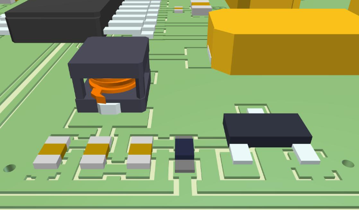
Switch-side PCBs, commonly found in power electronics, require careful attention to copper pour design due to high current flows, rapid switching transitions, and thermal constraints. Copper pours—large areas of conductive copper—serve multiple purposes, including:
- Current Carrying Capacity: Reducing trace resistance to minimize power losses.
- Thermal Management: Dissipating heat from high-power components.
- Signal Integrity: Providing low-impedance return paths for high-frequency signals.
- EMI Reduction: Shielding sensitive circuits from noise.
This paper discusses design strategies for optimizing copper pours in switch-side PCBs.
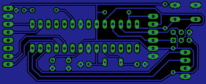
2. Copper Pour Techniques
2.1 Solid vs. Hatched Copper Pour
- Solid Copper Pour: Offers the lowest resistance and best thermal conductivity, ideal for high-current paths. However, it may lead to PCB warping due to uneven thermal expansion.
- Hatched Copper Pour: Reduces copper usage and minimizes warping but increases resistance. Suitable for lower-current applications where mechanical stability is a priority.
2.2 Copper Thickness Considerations
The thickness of copper (measured in ounces per square foot, e.g., 1 oz, 2 oz) impacts current handling and thermal performance:
- 1 oz (35 µm): Standard for low-power circuits.
- 2 oz (70 µm) or higher: Preferred for high-current switch-side PCBs to reduce resistive losses.
2.3 Copper Pour and Current Density
Copper pours must handle peak current without excessive heating. The current-carrying capacity can be estimated using IPC-2152 standards. Wider pours or thicker copper layers are necessary for high-current paths.
3. Thermal Management with Copper Pour
3.1 Heat Dissipation
Copper’s high thermal conductivity helps transfer heat away from power components (MOSFETs, diodes, inductors). Key strategies include:
- Thermal Relief Pads: Prevent excessive heat sinking during soldering while maintaining electrical connectivity.
- Copper Fills Under Components: Enhances heat spreading but must avoid solderability issues.
3.2 Via Arrays for Heat Transfer
Thermal vias beneath high-power components improve heat dissipation to inner layers or the opposite side of the PCB. A grid of vias (e.g., 0.3 mm diameter, 1 mm pitch) is commonly used.

4. Grounding and EMI Mitigation
4.1 Ground Plane Design
A solid ground plane beneath high-speed switching traces minimizes loop inductance and reduces EMI. Key considerations:
- Avoid Split Grounds: Prevents ground loops and noise coupling.
- Star Grounding for Mixed Signals: Separates analog and digital grounds at a single point.
4.2 High-Frequency Considerations
Fast-switching signals (e.g., in buck/boost converters) generate high-frequency noise. Techniques to mitigate EMI include:
- Return Path Optimization: Ensure uninterrupted copper pour beneath high-speed traces.
- Edge Shielding: Adding grounded copper along PCB edges to reduce radiated emissions.
5. Practical Implementation Guidelines
5.1 Component Placement and Copper Pour
- Place high-current components (MOSFETs, inductors) close to minimize loop area.
- Use copper pours to connect power components directly, reducing parasitic inductance.
5.2 Avoiding Copper Pour Issues
- Acid Traps: Narrow copper slivers can etch unevenly, leading to manufacturing defects.
- Starvation Areas: Ensure sufficient copper around high-current traces to prevent overheating.
5.3 Simulation and Verification
- Thermal Simulation: Tools like Ansys Icepak or SolidWorks Flow Simulation predict hot spots.
- EMI Analysis: Use tools such as Keysight ADS or CST Studio Suite to evaluate radiated noise.
6. Case Study: DC-DC Converter PCB
A 12V-to-5V buck converter was designed with:
- 2 oz copper pour for power traces
- Thermal vias under the MOSFET
- Solid ground plane beneath switching nodes
Results showed a 15% reduction in temperature rise and 20% lower EMI emissions compared to a non-optimized layout.
7. Conclusion
Effective copper pour design in switch-side PCBs enhances performance, reliability, and manufacturability. Key takeaways:
- Use solid copper pours for high-current paths and hatched fills where mechanical stability is critical.
- Optimize thermal vias and copper thickness for heat dissipation.
- Maintain low-impedance ground paths to minimize EMI.
- Validate designs through simulation and prototyping.
By following these guidelines, engineers can achieve robust switch-side PCB layouts suitable for demanding power electronics applications.