Parametric Constraints in PCB Design: Enhancing Efficiency and Precision
Introduction
Printed Circuit Board (PCB) design has evolved significantly over the past decades, transitioning from manual drafting to sophisticated computer-aided design systems. One of the most impactful advancements in modern PCB design tools is the implementation of parametric constraints—a systematic approach that allows designers to define and manage design rules through mathematical relationships and logical conditions. This 2000-word article explores the concept, implementation, and benefits of using parametric constraints in PCB design, demonstrating how this methodology improves design quality, accelerates development cycles, and facilitates design reuse.
Understanding Parametric Constraints
Parametric constraints in PCB design refer to the practice of defining design elements and their relationships through mathematical parameters and rules rather than fixed values. These constraints create dynamic relationships between various components, traces, vias, and other board elements, enabling automatic adjustments when changes occur in the design.
At its core, parametric design establishes relationships such as:
- Trace width being a function of current requirements
- Component spacing determined by manufacturing capabilities
- Via sizes related to their purpose (signal, power, or ground)
- Layer stackup dimensions based on impedance requirements
This approach contrasts with traditional static design methods where each element is defined independently, requiring manual updates when changes are necessary.

Types of Parametric Constraints in PCB Design
Modern PCB design tools offer several categories of parametric constraints:
1. Electrical Constraints
These ensure the design meets signal integrity requirements:
- Impedance control (single-ended and differential pairs)
- Propagation delay matching (length tuning)
- Crosstalk limitations
- Current carrying capacity rules
2. Physical Constraints
These govern the physical layout characteristics:
- Minimum/maximum trace widths
- Clearance rules (conductor-to-conductor, conductor-to-pad)
- Solder mask expansion values
- Silkscreen requirements
3. Manufacturing Constraints
Parameters that ensure manufacturability:
- Drill size limitations
- Annular ring requirements
- Copper-to-edge spacing
- Solder paste mask definitions
4. Assembly Constraints
Rules affecting component placement and orientation:
- Component-to-component spacing
- Placement keepouts
- Orientation requirements for automated assembly
5. High-Speed Design Constraints
Specialized rules for high-frequency designs:
- Matched length groups
- Phase tolerance requirements
- Differential pair skew limits
Implementing Parametric Constraints
Effective implementation of parametric constraints requires a systematic approach:
1. Constraint Definition
Designers begin by identifying the key parameters that will drive the design. These typically include:
- Board dimensions and layer stackup
- Component libraries with parametric footprints
- Design rule templates for different circuit types (digital, analog, RF, power)
2. Constraint Hierarchy Establishment
Constraints are organized in a hierarchical structure:
- Global constraints (apply to entire board)
- Net class constraints (group-specific rules)
- Net-specific constraints (individual net requirements)
- Component class constraints
- Component-specific constraints
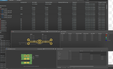
3. Constraint Management
Advanced PCB tools provide constraint managers that:
- Display all active constraints
- Highlight conflicts
- Allow for constraint prioritization
- Enable constraint inheritance and override capabilities
4. Constraint Validation
Real-time design rule checking (DRC) ensures compliance throughout the design process, rather than just at final verification.
Benefits of Parametric Constraint-Based Design
The adoption of parametric constraints offers numerous advantages:
1. Design Consistency
Parametric constraints enforce uniform application of design rules across the entire board, eliminating human error in manual rule application. This is particularly valuable in large designs with multiple team members working on different sections.
2. Design Automation
Many routine design tasks can be automated through parametric rules:
- Automatic trace width adjustment based on current requirements
- Dynamic via selection based on net characteristics
- Intelligent component placement respecting thermal and mechanical constraints
3. Design Reuse and Scalability
Parametric designs are inherently more reusable because constraints can be saved as templates and applied to new designs. This is especially valuable for:
- Product families with varying sizes or capabilities
- Technology platforms that evolve over multiple generations
- Design blocks that are reused across projects
4. Improved Design Quality
Constraint-driven design catches potential issues early in the process:
- Signal integrity problems are prevented through proper impedance control
- Manufacturing issues are avoided by enforcing fabrication rules
- Assembly problems are minimized through proper component placement rules
5. Faster Design Iterations
When changes are required, parametric constraints automatically propagate modifications throughout the design:
- Board outline changes automatically adjust keepout areas
- Layer stackup modifications update impedance-controlled traces
- Component swaps automatically update footprint and routing requirements
6. Better Documentation
Parametric constraints serve as living documentation of design intent:
- Constraints explicitly capture design requirements
- Rule hierarchies document priority decisions
- Constraint templates preserve organizational knowledge
Advanced Applications of Parametric Constraints
1. Multi-board Systems
Parametric constraints extend beyond single PCBs to manage:
- Inter-board connections and alignment
- Enclosure and mechanical interface requirements
- System-level signal integrity considerations
2. Design for Manufacturing (DFM)
Advanced constraint systems incorporate:
- Manufacturer-specific capability profiles
- Process-specific design rules
- Yield optimization parameters
3. Thermal Management
Parametric approaches enable:
- Dynamic copper pour definitions based on thermal requirements
- Component spacing rules considering thermal dissipation
- Via patterns adjusted for optimal heat transfer
4. Flex and Rigid-Flex Designs
Specialized constraints handle:
- Bend radius requirements
- Transition zone management
- Flexible section routing rules
Best Practices for Parametric Constraint Implementation
To maximize the benefits of parametric constraints, designers should:
- Start with Standards: Begin with industry-standard design rules before adding project-specific constraints.
- Organize Constraints Logically: Create a clear hierarchy from global to specific constraints.
- Document Constraint Rationale: Record why each constraint exists to aid future modifications.
- Validate Constraint Sets: Test constraint templates on sample designs before full implementation.
- Balance Strictness and Flexibility: Avoid over-constraining designs where flexibility is needed.
- Regularly Update Constraints: Maintain constraints as technologies and requirements evolve.
Challenges and Considerations
While parametric constraints offer significant advantages, some challenges exist:
- Initial Setup Time: Developing comprehensive constraint sets requires upfront investment.
- Learning Curve: Design teams need training to work effectively with constraint systems.
- Over-Constraint Risks: Excessive constraints can limit design flexibility unnecessarily.
- Tool Limitations: Not all PCB tools offer equally sophisticated constraint management.
- Performance Impacts: Complex constraint systems may slow down design tools.
Future Trends in Parametric PCB Design
The future of parametric constraints in PCB design includes:
- AI-Assisted Constraint Generation: Machine learning algorithms suggesting optimal constraints based on design goals.
- Cloud-Based Constraint Libraries: Shared repositories of verified constraint templates.
- Multi-Physics Constraints: Integrated electrical, thermal, and mechanical rule systems.
- Generative Design Integration: Automated design exploration within constraint boundaries.
- Real-Time Manufacturing Feedback: Direct links between constraint systems and manufacturer capabilities.
Conclusion
Parametric constraint-based design represents a fundamental shift in PCB development methodology, moving from static, manual design processes to dynamic, rule-driven systems. By capturing design intent and requirements as formal constraints, engineers can create higher quality boards more efficiently while enabling design reuse and automation. As PCB technologies continue to advance in complexity—with higher speeds, denser layouts, and more challenging manufacturing requirements—the strategic use of parametric constraints will become increasingly essential for successful electronic product development.
The implementation of parametric constraints does require thoughtful planning and investment in design methodology, but the long-term benefits in quality, efficiency, and reliability make it a compelling approach for any organization serious about PCB design excellence. As tools continue to evolve, we can expect parametric constraint systems to become even more sophisticated, further empowering designers to meet the ever-growing challenges of modern electronics design.