High-Density Interconnect (HDI) PCBs vs. Conventional PCBs: A Comprehensive Comparison
Introduction
Printed Circuit Boards (PCBs) form the backbone of modern electronics, providing the physical platform for component mounting and electrical connections. As electronic devices continue to shrink in size while increasing in functionality, the demand for more sophisticated PCB technology has grown exponentially. This evolution has led to the development of High-Density Interconnect (HDI) PCBs, which offer significant advantages over conventional PCBs in many applications. This article explores the key characteristics that differentiate HDI technology from standard PCB approaches, examining their respective designs, manufacturing processes, performance capabilities, and application areas.
Fundamental Differences Between HDI and Conventional PCBs
Definition and Basic Construction
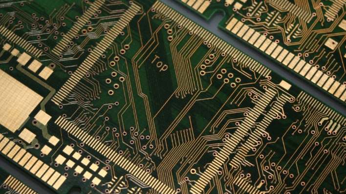
Conventional PCBs, also known as standard or traditional PCBs, typically feature a simpler design with fewer layers (often 1-8 layers), larger trace widths and spacing, and through-hole vias that span the entire board thickness. These boards have served the electronics industry well for decades and continue to be used in many applications where high density isn’t a critical requirement.
HDI PCBs, in contrast, represent an advanced PCB technology designed to accommodate more components in a smaller area. They achieve this through several key features:
- Microvias (typically less than 150 microns in diameter)
- Finer trace widths and spacing (often below 100 microns)
- Higher connection pad density
- Frequently employ blind and buried vias
- May incorporate multiple lamination cycles (sequential build-up)
Density Metrics
The primary differentiator between HDI and conventional PCBs lies in their interconnect density, which can be measured through several metrics:
- Line/Space Width: While conventional PCBs might have 100/100 μm (4/4 mil) as standard, HDI PCBs commonly achieve 50/50 μm or even smaller.
- Via Density: HDI allows for via densities exceeding 20 vias/cm², compared to perhaps 5-10 vias/cm² in conventional designs.
- Pad Density: HDI supports smaller component pitches, enabling more I/O connections per unit area.
Technical Characteristics Comparison
Miniaturization Capabilities
HDI technology enables unprecedented levels of miniaturization through several mechanisms:
Microvias: These small-diameter vias (typically laser-drilled) allow for connections between adjacent layers without consuming valuable real estate. Conventional PCBs use mechanically drilled through-vias that penetrate the entire board, limiting routing options.
Fine-Pitch Components: HDI supports chip-scale packages (CSP), ball grid arrays (BGAs) with fine pitches (0.4mm or less), and other advanced packaging technologies that would be impractical on conventional PCBs.
Reduced Layer Count for Equivalent Functionality: An HDI design might achieve the same functionality as a conventional PCB with 30-50% fewer layers, reducing thickness and weight.
Electrical Performance
The compact nature of HDI PCBs offers several electrical advantages:
Improved Signal Integrity: Shorter interconnect lengths reduce signal propagation delays and attenuation. The controlled impedance of fine traces in HDI can be more precisely managed.
Reduced Parasitics: Smaller vias and shorter traces decrease parasitic capacitance and inductance, crucial for high-frequency applications.
Better Power Distribution: The dense via arrangements in HDI allow for more effective power and ground distribution networks, reducing voltage drops and improving noise immunity.
Reliability Considerations
While both PCB types can be highly reliable when properly designed and manufactured, HDI presents unique characteristics:
Microvia Reliability: Properly constructed microvias demonstrate excellent reliability, often surpassing conventional through-hole vias in thermal cycling performance due to their smaller size and reduced z-axis expansion.
Material Selection: HDI often employs high-performance materials with better thermal and mechanical properties to accommodate the dense designs.
Thermal Management: The higher density of HDI can create thermal challenges, often requiring careful thermal design and sometimes incorporating thermal vias or other cooling solutions.
Manufacturing Process Differences
Fabrication Complexity
Conventional PCB manufacturing follows well-established processes:
- Panel preparation
- Drilling (mechanical)
- Plating
- Patterning (imaging and etching)
- Lamination (for multilayer)
- Surface finish
- Testing
HDI manufacturing adds several complex steps:
- Laser drilling for microvias
- Sequential lamination cycles
- Via filling and planarization
- More precise imaging processes (often using LDI – Laser Direct Imaging)
- Advanced inspection techniques (AOI, microsection analysis)
Material Requirements
While conventional PCBs often use standard FR-4 materials, HDI PCBs frequently require:
- Low-profile copper foils
- High-performance laminates with better dimensional stability
- Thin dielectric materials for layer separation
- Specialized via fill materials
Yield and Cost Factors
HDI manufacturing typically has lower yields initially due to the precision required, leading to higher costs. However, as the technology matures and processes improve, this gap narrows. Conventional PCBs benefit from decades of process optimization that keep costs relatively low for standard designs.
Design Considerations
Layout Strategies
Conventional PCB design follows more straightforward rules:
- Larger clearances
- Simpler via strategies
- More generous design rules
- Often manual routing is feasible
HDI design requires advanced techniques:
- Extensive use of via-in-pad
- Complex stackup planning
- High-density routing strategies
- Typically requires advanced EDA tools with HDI capabilities
- Often employs autorouting for dense areas
Design Rule Checking
HDI demands much stricter design rule checks (DRC) for:
- Annular ring requirements
- Via-to-via spacing
- Microvia aspect ratios
- Copper balance for lamination
- Impedance control on fine features
Application Areas
Conventional PCB Applications
Standard PCBs continue to dominate in:
- Consumer appliances
- Basic electronics
- Power electronics
- Industrial controls
- Automotive non-critical systems
- Applications where cost is the primary driver
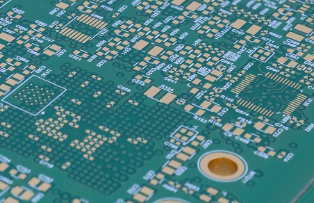
HDI PCB Applications
HDI technology enables advanced applications:
- Smartphones and tablets
- Wearable electronics
- Medical imaging devices
- Aerospace and defense systems
- High-performance computing
- Advanced automotive electronics (ADAS, infotainment)
- IoT devices requiring compact form factors
Cost-Benefit Analysis
While HDI PCBs typically carry a higher initial cost, they can provide significant system-level benefits:
- Size Reduction: Enables smaller end products with competitive advantages
- Improved Performance: Better signal integrity for high-speed designs
- Reliability: Often more reliable in demanding environments
- Assembly Benefits: Can simplify component placement and reduce assembly defects
- Material Efficiency: May use less raw material despite higher processing costs
The decision between HDI and conventional PCBs ultimately depends on the specific application requirements, with HDI justifying its premium in applications where miniaturization, performance, or reliability are critical.
Future Trends
The PCB industry continues to evolve, with several trends affecting both conventional and HDI technologies:
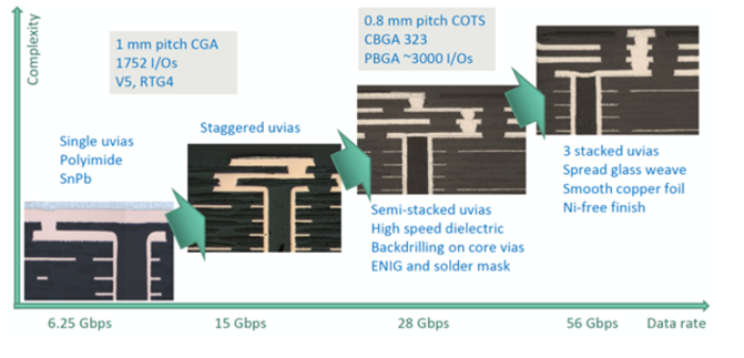
- Further Miniaturization: HDI features continue to shrink, with line/space moving toward 20/20 μm
- Embedded Components: More passive (and eventually active) components being embedded within the PCB
- Advanced Materials: Development of materials with better high-frequency performance
- Additive Processes: Increased use of inkjet and other additive manufacturing techniques
- Sustainability: More focus on recyclable materials and environmentally friendly processes
Conclusion
HDI PCB technology represents a significant advancement over conventional PCB approaches, offering superior density, performance, and miniaturization capabilities. While conventional PCBs remain appropriate for many applications, HDI has become essential for cutting-edge electronics where space constraints, high-speed performance, or advanced packaging requirements exist. The choice between these technologies involves careful consideration of technical requirements, cost factors, and manufacturing capabilities. As electronic devices continue their trend toward greater functionality in smaller packages, HDI technology will likely see expanded adoption across an increasing range of applications, while conventional PCBs will maintain their position in cost-sensitive or less demanding applications. Understanding the characteristics and capabilities of both approaches enables engineers to make informed design decisions that optimize performance, reliability, and cost-effectiveness for their specific applications.