Why Do PCBs Warp and How to Prevent It?
Introduction
Printed Circuit Boards (PCBs) are fundamental components in modern electronics, serving as the backbone for virtually all electronic devices. However, one of the most common and frustrating issues in PCB manufacturing and assembly is warping – the undesired bending or twisting of the board. This phenomenon can lead to significant problems in both manufacturing processes and final product performance. Understanding why PCBs warp and how to prevent it is crucial for electronics manufacturers, designers, and engineers.
This article will explore the root causes of PCB warping, examine its consequences, and provide comprehensive strategies to minimize or eliminate this problem throughout the PCB lifecycle – from design and material selection to manufacturing and assembly processes.
Understanding PCB Warping
Definition and Types of Warping
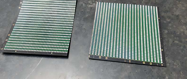
PCB warping refers to the deformation of a circuit board from its intended flat shape. This deformation can take several forms:
- Bow: A curvature across the length or width of the board where the four corners remain in the same plane
- Twist: A three-dimensional deformation where one corner is not in the same plane as the other three
- Bend: A combination of bow and twist that creates complex deformations
Measurement Standards
The industry standard for measuring warpage is IPC-A-600, which defines acceptable levels of warping based on board thickness:
- For boards ≤ 0.8mm thick: maximum 0.75% warpage
- For boards > 0.8mm thick: maximum 0.50% warpage
Warpage percentage is calculated as:
Warpage % = (Maximum Deflection / Board Length) × 100Root Causes of PCB Warping
1. Material Selection and Properties
The choice of base materials significantly impacts a PCB’s tendency to warp:
Coefficient of Thermal Expansion (CTE) Mismatch
- Different materials in the PCB stackup (copper, FR-4, prepreg) expand at different rates when heated
- The typical CTE for:
- Copper: ~17 ppm/°C
- FR-4 in X/Y axis: ~12-16 ppm/°C
- FR-4 in Z axis: ~50-70 ppm/°C
- This mismatch creates internal stresses that can lead to warping
Material Quality and Consistency
- Variations in resin content or glass weave pattern in the substrate
- Inconsistent curing of prepreg materials
- Moisture absorption in hygroscopic materials
2. Design Factors
Asymmetric Stackup
- Uneven copper distribution between layers
- Different copper weights on opposite sides
- Odd number of layers without proper balancing
Board Geometry
- Large, thin boards are more prone to warping
- Irregular shapes or cutouts can create stress concentration points
Copper Distribution
- Large copper pours on one side without balancing on the opposite side
- Significant differences in copper density between layers
3. Manufacturing Processes
Lamination Process
- Improper temperature and pressure profiles during lamination
- Uneven cooling rates after lamination
- Residual stresses from the curing process
Drilling and Routing
- Mechanical stresses induced during drilling operations
- Heat generation during routing operations
- Improper handling after machining
Copper Plating
- Uneven copper deposition creating mechanical stresses
- Electroplating processes that introduce internal stresses
4. Environmental Factors
Temperature Variations
- Exposure to high temperatures during assembly (especially reflow soldering)
- Thermal cycling during operation
- Storage in high-temperature environments
Moisture Absorption
- Most PCB substrate materials absorb moisture from the environment
- Rapid heating causes moisture to expand, potentially warping the board
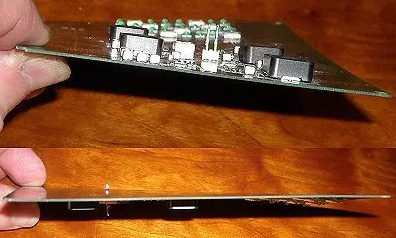
Consequences of PCB Warping
Manufacturing Challenges
- Assembly Difficulties:
- Component placement accuracy issues
- Poor solder paste deposition
- Tombstoning of small components
- Soldering Problems:
- Poor wetting and solder joint formation
- Head-in-pillow defects in BGA packages
- Open connections or bridges
- Automated Handling Issues:
- Pick-and-place machine feeding problems
- Conveyor system jams
- Vision system alignment failures
Reliability Concerns
- Mechanical Stress on Components:
- Cracked solder joints
- Delamination of components
- Stress on wire bonds in IC packages
- Long-Term Performance:
- Increased susceptibility to thermal cycling failures
- Potential for intermittent connections
- Reduced product lifespan
- Final Product Integration:
- Difficulties in enclosure fitting
- Stress on connectors and mechanical interfaces
- Potential for short circuits in tight assemblies
Prevention Strategies
1. Design Considerations
Balanced Stackup Design
- Maintain symmetry in layer stackup (same copper weights and patterns on mirrored layers)
- For odd layer counts, add dummy copper layers to maintain balance
- Keep similar dielectric thicknesses on either side of the center layer
Copper Distribution Optimization
- Use hatched copper pours instead of solid when possible
- Balance copper density across layers (aim for <30% difference between sides)
- Add thieving copper in sparse areas to maintain balance
Board Geometry Planning
- Avoid extremely thin boards for large designs (minimum 1.6mm recommended for boards >150mm)
- Use rounded corners instead of sharp angles
- Consider adding stiffeners or support frames for large boards
2. Material Selection
Substrate Material Choices
- High-Tg materials (Tg > 170°C) for improved thermal stability
- Low-CTE materials for reduced thermal expansion effects
- Consider specialized materials like polyimide for flexible applications
Copper Foil Considerations
- Use rolled annealed copper for better mechanical properties
- Consider reverse-treated foils for improved adhesion
- Balance copper weights across layers
Prepreg Selection
- Match resin content to application requirements
- Consider low-flow prepregs for better dimensional stability
- Ensure consistent glass weave styles throughout the stackup
3. Manufacturing Process Controls
Lamination Process Optimization
- Implement controlled ramp-up and cool-down rates (typically 2-3°C/min)
- Use balanced pressure profiles during lamination
- Consider multi-stage lamination for complex boards
Drilling and Routing Best Practices
- Use sharp drill bits and proper feed rates
- Implement step drilling for high aspect ratio holes
- Allow adequate time for heat dissipation between operations
Post-Manufacturing Conditioning
- Implement controlled cooling after hot processes
- Consider stress-relief baking (typically 120-150°C for 4-6 hours)
- Proper storage in controlled environments
4. Assembly Process Considerations
Pre-Baking Protocols
- Bake moisture-sensitive boards before assembly (typically 105-125°C for 2-8 hours)
- Follow IPC-1601 guidelines for handling moisture-sensitive PCBs
- Use dry storage for baked boards
Reflow Profile Optimization
- Use gradual temperature ramps (1-2°C/sec)
- Ensure even heating across the board
- Consider forced convection ovens for large boards
Fixture and Support Usage
- Use pallets or carriers for thin boards during assembly
- Implement support pins in reflow ovens
- Consider vacuum fixtures for critical applications
Advanced Solutions for Warpage Control
1. Engineering Solutions
Embedded Components
- Reduces the need for surface mount components that can create imbalances
- Provides more uniform thermal mass distribution
Metal Core PCBs
- Aluminum or copper cores provide excellent dimensional stability
- Particularly effective for high-power applications
Stiffener Implementation
- Aluminum or stainless steel stiffeners for flexible circuits
- Localized reinforcement for critical areas
2. Process Innovations
Sequential Lamination
- Breaks complex stackups into simpler, more balanced sub-assemblies
- Allows for better stress management
Low-Stress Plating
- Pulse plating techniques for more uniform deposition
- Additives that reduce internal plating stresses
Laser Direct Imaging
- Reduces mechanical stresses compared to traditional photolithography
- Enables finer feature control
Testing and Quality Control
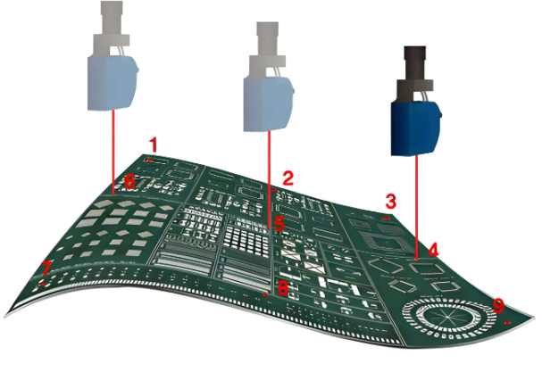
Warpage Measurement Techniques
- Shadow Moiré:
- Non-contact optical method
- Provides full-field warpage data
- Excellent for measuring dynamic warpage during thermal cycling
- Laser Scanning:
- High-precision surface mapping
- Suitable for both bare and assembled boards
- Coordinate Measuring Machines (CMM):
- Contact-based measurement
- High accuracy for small areas
Process Monitoring
- In-line Inspection:
- Automated optical inspection (AOI) for warpage detection
- Real-time monitoring during critical processes
- Statistical Process Control:
- Track warpage trends over time
- Identify process drift before it causes failures
- Thermal Profiling:
- Monitor actual temperature exposure during lamination and assembly
- Ensure consistent process conditions
Conclusion
PCB warping is a complex phenomenon resulting from the interplay of material properties, design decisions, manufacturing processes, and environmental factors. While complete elimination of warpage may not always be possible, understanding its root causes and implementing comprehensive prevention strategies can significantly reduce its occurrence and impact.
The key to successful warpage management lies in a holistic approach that considers the entire PCB lifecycle – from initial material selection and design through manufacturing and assembly. By implementing balanced designs, carefully controlling processes, and employing appropriate quality control measures, manufacturers can produce flat, reliable PCBs that meet the demanding requirements of modern electronics.
As PCB technology continues to evolve with thinner substrates, higher component densities, and more challenging operating environments, the importance of warpage control will only increase. Staying informed about new materials, processes, and analysis techniques will be essential for maintaining high yields and reliable products in this ever-changing landscape.