Can PCB Parasitic Components Be Simulated? An In-Depth Analysis
Introduction
Printed Circuit Boards (PCBs) are fundamental to modern electronics, providing the physical platform for interconnecting electronic components. However, as signal frequencies increase and device sizes shrink, parasitic components—unintended inductances, capacitances, and resistances—become increasingly significant. These parasitics can degrade signal integrity, cause electromagnetic interference (EMI), and lead to unexpected circuit behavior.
A critical question in PCB design is whether these parasitic components can be accurately simulated before fabrication. This article explores the feasibility, methods, and challenges of simulating PCB parasitic elements.
Understanding PCB Parasitic Components
Parasitic components in PCBs are unintended electrical properties that arise due to physical layout characteristics. The three primary types are:
- Parasitic Capacitance (C): Occurs between two conductive traces, planes, or components separated by an insulating material (dielectric). High-frequency signals can couple unintentionally due to this capacitance.
- Parasitic Inductance (L): Results from current flowing through conductive traces, especially in loops or long paths. This inductance can cause voltage spikes and ringing in high-speed circuits.
- Parasitic Resistance (R): The inherent resistance of PCB traces, which can lead to voltage drops and power losses, particularly in high-current applications.
These parasitics are influenced by trace geometry, material properties, and proximity effects, making them difficult to eliminate entirely. However, simulation tools can help predict and mitigate their impact.
Simulation of PCB Parasitic Components
Yes, PCB parasitic components can be simulated using various software tools and techniques. The accuracy of these simulations depends on the modeling approach, software capabilities, and the designer’s understanding of parasitic effects.
1. Simulation Methods
Several simulation techniques are used to analyze parasitics in PCBs:
A. Electromagnetic Field Solvers
- Finite Element Method (FEM): Solves Maxwell’s equations numerically, providing high accuracy for complex geometries. Tools like ANSYS HFSS and COMSOL Multiphysics use FEM.
- Method of Moments (MoM): Efficient for planar structures, used in tools like Keysight ADS and Sonnet.
- Finite Difference Time Domain (FDTD): Simulates time-domain behavior, useful for transient analysis (e.g., CST Studio Suite).
These solvers extract parasitic capacitance, inductance, and resistance by modeling the electromagnetic interactions between conductors and dielectrics.
B. Lumped-Element Equivalent Models
- For simpler structures, parasitic effects can be approximated using lumped RLC (resistor-inductor-capacitor) models.
- SPICE-based simulators (e.g., LTspice, PSpice) allow designers to insert parasitic values manually or extract them from field solvers.
C. Transmission Line Modeling
- High-speed signals require transmission line analysis to account for impedance mismatches and reflections.
- Tools like HyperLynx (Siemens) and Sigrity (Cadence) specialize in signal integrity simulations, including parasitic effects.
2. Simulation Workflow
A typical parasitic simulation workflow involves:
- PCB Layout Import: Load the design into the simulation tool (e.g., from Altium, KiCad, or Cadence Allegro).
- Material and Stack-up Definition: Specify dielectric constants, copper thickness, and layer arrangements.
- Parasitic Extraction: Use field solvers to compute parasitic RLC values.
- Post-Processing: Analyze results, identify critical parasitics, and optimize the design.
- Validation: Compare simulations with real-world measurements (if possible).
3. Challenges in Parasitic Simulation
While simulation is powerful, several challenges exist:
- Computational Complexity: Full-wave 3D simulations are resource-intensive and time-consuming.
- Model Accuracy: Simplified models may overlook coupling effects between distant traces.
- Frequency-Dependent Effects: Parasitics vary with frequency, requiring broadband simulations.
- Manufacturing Variations: PCB fabrication tolerances (e.g., dielectric thickness, copper roughness) affect parasitics but are hard to model precisely.
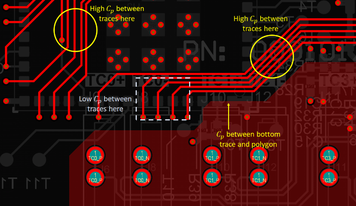
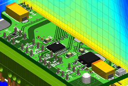
Case Study: Simulating Parasitic Capacitance in a High-Speed PCB
Consider a high-speed digital design where crosstalk between adjacent traces is a concern. Using ANSYS HFSS:
- The PCB layout is imported, and the critical signal traces are selected.
- A 3D electromagnetic simulation is run to extract parasitic capacitance between the traces.
- The results show a capacitance of 0.5 pF, which could cause signal integrity issues above 1 GHz.
- The designer adjusts trace spacing and adds ground shielding to reduce the parasitic effect.
- A follow-up simulation confirms the improvement.
This example demonstrates how simulation helps optimize PCB performance before fabrication.
Conclusion
PCB parasitic components can indeed be simulated using advanced electromagnetic solvers, lumped-element models, and signal integrity tools. While challenges such as computational complexity and model accuracy persist, modern simulation techniques provide valuable insights that help mitigate parasitic effects early in the design phase.
As PCB technology advances toward higher frequencies and miniaturization, the role of parasitic simulation will only grow in importance. By leveraging these tools, engineers can design more reliable and high-performance electronic systems.