How to Design a PCB That Can Handle 100A Current
Introduction
Printed Circuit Boards (PCBs) are the backbone of modern electronics, but when it comes to high-current applications like power supplies, motor controllers, or industrial equipment, standard PCB designs fall short. Designing a PCB that can reliably handle 100 amps requires careful consideration of multiple factors including trace width, copper weight, thermal management, and material selection. This article provides a comprehensive guide to creating robust PCBs capable of sustaining 100A currents without failure.
Understanding Current Carrying Capacity
Current and Heat Relationship
The fundamental challenge with high-current PCBs is heat generation. When current flows through a conductor, it encounters resistance which converts electrical energy into thermal energy (heat) according to Joule’s law (P = I²R). At 100A, even small resistances can generate substantial heat:
- A mere 1mΩ resistance at 100A produces 10W of heat (P = 100² × 0.001)
- This heat must be effectively dissipated to prevent thermal damage
Factors Affecting Current Capacity
Several key factors determine how much current a PCB trace can handle:
- Trace cross-sectional area (width × thickness)
- Copper weight (thickness)
- Ambient temperature
- Allowed temperature rise
- PCB material thermal conductivity
- Presence of cooling mechanisms
- Duration of current flow (continuous vs. pulsed)
Trace Design for 100A Currents
Calculating Required Trace Width
The IPC-2152 standard provides the most accurate method for determining appropriate trace widths. For 100A applications:
- Determine your acceptable temperature rise (typically 10°C-20°C for high current)
- Select copper weight (common choices are 2oz/ft² to 6oz/ft²)
- Use IPC-2152 charts or calculators to find required width
Example Calculation:
- Current: 100A
- Copper weight: 4oz/ft² (140μm thick)
- Temperature rise: 20°C
- Required width: ~100mm (internal layer) or ~75mm (external layer)
Note: These are approximate values—always perform detailed calculations for your specific application.
Practical Trace Design Strategies
Given that 100mm wide traces are often impractical, consider these alternatives:
- Multiple parallel traces:
- Use several narrower traces in parallel
- Ensure equal length to prevent current imbalance
- Connect at multiple points
- Copper pours instead of traces:
- Create large copper areas for current paths
- Often more space-efficient than extremely wide traces
- Multi-layer current sharing:
- Route current across multiple layers
- Use plenty of vias to connect layers
Copper Weight and Thickness
Standard PCBs use 1oz/ft² (35μm) copper, but this is inadequate for 100A:
| Copper Weight | Thickness | Relative Current Capacity |
|---|---|---|
| 1oz/ft² | 35μm | 1× (base reference) |
| 2oz/ft² | 70μm | ~1.8× |
| 3oz/ft² | 105μm | ~2.5× |
| 4oz/ft² | 140μm | ~3.2× |
| 6oz/ft² | 210μm | ~4.5× |
For 100A applications:
- Minimum recommendation: 4oz/ft² copper
- Preferred: 6oz/ft² or heavier
- Extreme cases: Consider copper up to 20oz/ft²
Via Design for High Current
Vias are critical bottlenecks in high-current paths. Standard via arrays can’t handle 100A:
- Via current capacity:
- A typical 0.3mm via can carry ~1A
- 100A would require ~100 vias (impractical)
- High-current via solutions:
- Large diameter vias: Use 0.5mm-1mm diameter vias
- Via stitching: Multiple vias in parallel
- Filled vias: Electrically and thermally conductive fill
- Copper plugs: Solid copper-filled vias
- Thermal vias:
- Help transfer heat to other layers or heatsinks
- Place in high-current areas even if not needed electrically
Thermal Management
Effective heat dissipation is crucial for reliability:
- PCB Material Selection:
- Standard FR-4 (TG130-TG170) works for moderate currents
- For 100A, consider:
- High-TG FR-4 (TG180+)
- Metal-core PCBs (aluminum or copper base)
- Ceramic substrates (for extreme cases)
- Insulated Metal Substrates (IMS)
- Heatsinking Strategies:
- Attach heatsinks to high-current areas
- Use thermal interface materials (TIMs)
- Consider forced air cooling for continuous 100A operation
- Temperature Monitoring:
- Include temperature sensors near high-current traces
- Implement thermal shutdown protection
Connector and Component Considerations
High-Current Connectors
- Selection criteria:
- Rated for >100A continuous current
- Low contact resistance (<0.5mΩ)
- Robust mechanical design
- Options:
- Anderson Power Poles
- Bulgin high-current connectors
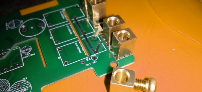
- Custom busbar interfaces
- Welded or soldered connections
Component Placement
- Minimize current path length:
- Place high-current components close together
- Avoid unnecessary bends or turns
- Termination methods:
- Use heavy gauge wire connections
- Consider busbars for very high currents
- Implement proper strain relief
Manufacturing Considerations
PCB Fabrication
- Copper uniformity:
- Ensure even copper distribution
- Specify minimum copper thickness requirements
- Plating requirements:
- Thicker copper plating in vias
- Consider ENEPIG or other premium finishes
- Tolerances:
- Tight control over etch compensation
- Minimal undercutting of thick copper
Assembly Processes
- Soldering challenges:
- Thick copper heatsinks components during soldering
- May require higher temperature profiles
- Alternative connections:
- Consider welding for very high currents
- Use conductive adhesives where appropriate
Testing and Validation
Electrical Testing
- Resistance measurement:
- Verify milliohm-level resistances
- Use 4-wire Kelvin measurement
- Current testing:
- Gradually ramp up to 100A
- Monitor temperature rise
- Voltage drop verification:
- Measure at full current
- Ensure acceptable power loss
Thermal Testing
- Infrared thermography:
- Identify hot spots
- Verify even current distribution
- Long-term reliability testing:
- Thermal cycling
- Continuous operation testing
Advanced Techniques for Extreme Currents
When standard PCB approaches are insufficient:
- Embedded busbars:
- Incorporate solid metal conductors within PCB
- Copper or aluminum bars for main current paths
- Hybrid designs:
- Combine PCB with busbar assemblies
- Use PCB for control, busbars for power
- 3D printed electronics:
- Emerging technology for custom high-current paths
- Allows innovative cooling solutions
Safety Considerations
- Clearance and creepage:
- Maintain proper spacing for high-current traces
- Consider potting or conformal coating
- Fault protection:
- Implement fast-acting fuses or circuit breakers
- Consider current-limiting designs
- Mechanical robustness:
- Ensure traces can withstand vibration
- Prevent mechanical stress on high-current joints
Conclusion
Designing a PCB to handle 100A currents requires a holistic approach that considers electrical, thermal, and mechanical factors. Key takeaways include:
- Use heavy copper (4oz/ft² minimum, 6oz/ft² preferred)
- Implement wide traces or copper pours (50-100mm equivalent)
- Employ multiple parallel vias for layer transitions
- Select appropriate substrate materials (high-TG or metal-core)
- Incorporate effective thermal management solutions
- Use high-quality connectors rated for the current
- Validate designs through rigorous testing
By carefully addressing each of these aspects, designers can create PCBs that reliably handle 100A currents while maintaining long-term reliability and safety. Remember that high-current PCB design often requires iteration—prototype early and test thoroughly to ensure your design meets all requirements.