How to Add Images to a PCB: A Comprehensive Guide
Introduction
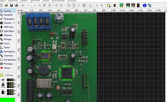
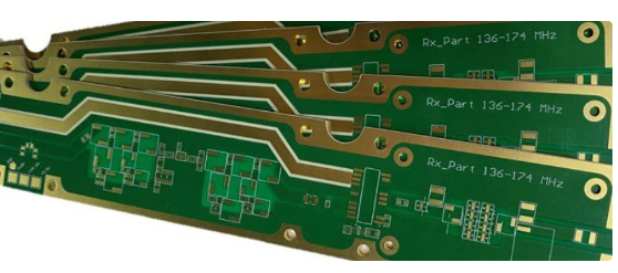
Printed Circuit Board (PCB) design has evolved significantly over the years, with designers now incorporating various graphical elements including logos, decorative patterns, and even functional images directly onto their boards. Adding images to PCBs serves multiple purposes – from branding and product identification to creating unique aesthetic designs or even embedding functional graphical elements like touchpad designs. This 2000-word guide will walk you through the complete process of adding images to your PCB designs, covering file preparation, conversion methods, placement techniques, and manufacturing considerations.

Understanding Image Requirements for PCBs
Before adding any image to your PCB, it’s crucial to understand the fundamental differences between standard digital images and PCB-compatible graphics:
- File Format Differences: PCBs require vector-based or monochrome raster images rather than typical RGB photographs
- Resolution Considerations: PCB images need to match your board’s manufacturing capabilities
- Color Representation: PCB images are typically represented by copper, silkscreen, or solder mask layers
- Manufacturing Constraints: Minimum line widths and spacing affect how detailed your image can be
Preparing Your Image File
Step 1: Choosing the Right Image
Select an image with:
- Clear, distinct features
- High contrast between elements
- Minimal fine details (unless working with high-precision manufacturing)
- Simple color schemes that can convert well to monochrome
Step 2: Image Conversion Methods
Method A: Vector Conversion (Recommended)
- Use vector graphic software (Adobe Illustrator, Inkscape, CorelDRAW)
- Trace or convert your image to vector format
- Simplify paths and reduce nodes where possible
- Save as SVG, DXF, or EPS format
Method B: Bitmap to Vector Conversion
- Use conversion tools like Inkscape’s Trace Bitmap function
- Adjust threshold and settings to capture essential details
- Clean up resulting vector paths
Method C: Direct Bitmap Use (For Simple Designs)
- Convert image to pure black and white (1-bit depth)
- Ensure resolution matches your PCB design requirements
- Save as BMP or PNG with transparency if needed

Importing Images into PCB Design Software
For Altium Designer Users:
- Place → Drawing Tools → Graphic
- Click to place image frame
- Browse and select your image file (supports BMP, JPG, PNG)
- Adjust properties like scale, layer, and position
For KiCad Users:
- Use the Bitmap2Component tool (under Tools menu)
- Import your image file
- Adjust settings (DPI, layer, negative/positive)
- Generate .kicad_mod file
- Import into PCB editor as a footprint
For Eagle Users:
- Use the ULP script “import-bmp.ulp”
- Select your image file
- Specify target layer and scaling
- Run the script to convert to vector elements
For OrCAD/Allegro Users:
- Use File → Import → DXF for vector graphics
- For bitmaps, convert to DXF first using external tools
- Adjust layer assignments during import
Layer Considerations for PCB Images
Decide which layer(s) to place your image on based on its purpose:
- Silkscreen Layer (Top/Bottom): For visible logos and text (typically white)
- Copper Layer: For conductive image elements (can be plated or unplated)
- Solder Mask Layer: Creates openings in the mask to expose copper beneath
- Paste Mask Layer: Rare, but can be used for special solder paste applications
Technical Considerations for PCB Images
- Minimum Line Width: Ensure all image features meet your manufacturer’s capabilities (typically 0.1mm/4mil for silkscreen)
- Clearance Requirements: Maintain proper spacing between image elements and other PCB features
- Scaling and Aspect Ratio: Verify final dimensions match your intended size
- File Size Impact: Complex images can significantly increase design file sizes
Advanced Techniques
Creating Custom Pad Shapes
- Convert image elements to pad shapes
- Assign proper net connections if needed
- Ensure proper spacing for solderability
Combining Images with Functional Elements
- Design touchpad interfaces using custom graphics
- Create decorative yet functional ground planes
- Incorporate images into board outlines or cutouts
Multi-layer Image Effects
- Combine silkscreen and exposed copper for two-tone effects
- Use solder mask color variations (if available)
- Create depth effects with multiple layer interactions
Manufacturing Considerations
- Discuss with Your Fabricator: Always verify image capabilities before finalizing design
- Silkscreen Limitations: Colors are typically limited to white or black
- Copper Image Options: Can be bare copper, plated, or covered with finish
- Special Processes: Some manufacturers offer specialized imaging like photo-realistic silkscreens
Troubleshooting Common Issues
- Pixelated or Low-Quality Images: Always start with highest resolution possible
- Missing Image Elements: Check layer visibility and object properties
- Manufacturing Defects: Ensure DPI/resolution matches board requirements
- File Import Failures: Try different formats or simplify complex vectors

Best Practices for PCB Images
- Keep it simple – complex images may not reproduce well
- Maintain adequate clearances around critical components
- Consider the viewing angle and orientation of the final product
- Use images purposefully – avoid cluttering functional areas
- Document image usage in your design notes
Alternative Approaches
- Direct PCB Printing: Some services offer full-color printing on boards
- Stickers/Labels: For low-volume applications where PCB imaging isn’t feasible
- Laser Marking: Post-production marking for serialization or customization
Conclusion
Adding images to PCBs has become an accessible feature for designers at all levels, offering new opportunities for branding, product differentiation, and even functional enhancements. By following the proper preparation, conversion, and placement techniques outlined in this guide, you can successfully incorporate images into your PCB designs while maintaining manufacturability and quality. Always remember to consult with your PCB manufacturer about their specific capabilities and requirements for imaging before finalizing your design.
With practice and attention to detail, PCB imaging can become a valuable tool in your design repertoire, helping create products that stand out both functionally and visually in the marketplace.


