PCB Design Pitfalls: The Often-Overlooked Issue of Hole Spacing
Introduction
In the intricate world of printed circuit board (PCB) design, engineers and designers must navigate a complex landscape of technical requirements, manufacturing constraints, and performance considerations. While much attention is rightly paid to trace routing, signal integrity, and component placement, one critical aspect frequently falls through the cracks: hole spacing. This seemingly simple element of PCB design can have profound implications for manufacturability, reliability, and functionality of the final product.
Hole spacing refers to the distance between drilled holes on a PCB, including via holes, component mounting holes, and through-hole component leads. Proper hole spacing affects everything from mechanical strength to electrical performance, yet it remains one of the most commonly overlooked aspects of PCB design. This article will explore why hole spacing matters, the consequences of improper spacing, and best practices to avoid these pitfalls in your designs.
The Importance of Proper Hole Spacing
Manufacturing Considerations
PCB fabrication involves precise drilling operations where even minor spacing violations can cause significant problems. Drill bits are physical tools that require adequate material between holes to maintain structural integrity of both the tool and the board. When holes are placed too close together:
- Drill Breakage Risk Increases: Small drill bits (especially those under 0.3mm) become fragile and prone to breakage when drilling near existing holes. Broken bits not only require machine stoppage for replacement but can also damage expensive production panels.
- Material Weakness Occurs: The web of material between closely spaced holes may be too thin to provide adequate mechanical support, leading to potential cracking during drilling, handling, or in-field use.
- Plating Problems Arise: Electroplating processes require sufficient space between holes to ensure proper copper deposition in the barrel of the via. Tight spacing can result in incomplete plating or voids that compromise reliability.
Electrical Performance Factors
Beyond manufacturing, hole spacing affects the electrical characteristics of the board:
- Impedance Control: Closely spaced vias can create impedance discontinuities in high-speed signals, particularly when they cluster near transmission lines.
- Crosstalk Potential: Insufficient spacing between via holes can allow electromagnetic coupling between signals, especially at higher frequencies.
- Current Carrying Capacity: Groups of closely spaced vias may create localized heating issues that affect current distribution and thermal management.
Mechanical Reliability Issues
The long-term durability of a PCB depends heavily on proper hole spacing:
- Thermal Stress: Different coefficients of thermal expansion between materials can cause stress concentrations in areas with dense hole patterns, potentially leading to cracking over temperature cycles.
- Vibration Resistance: Boards subject to mechanical vibration need adequate material between holes to prevent fatigue failure at stress points.
- Assembly Stress: During component insertion or press-fit operations, closely spaced holes may not provide enough support, leading to pad lifting or material damage.
Common Hole Spacing Pitfalls
Via-to-Via Spacing Neglect
Many designers focus on component placement but give little thought to via placement density. Common issues include:
- Via Barricades: Creating walls of vias for ground connections without considering spacing requirements
- Escape Routing: Crowding vias in breakout patterns from fine-pitch components
- Thermal Relief Patterns: Using too many closely spaced thermal vias under components
Component Hole Spacing Oversights
Through-hole components present their own spacing challenges:
- Lead-to-Lead Clearance: Not accounting for component body constraints versus hole placement
- Mounting Hardware Conflicts: Positioning mounting holes too close to component holes
- Wave Soldering Shadows: Dense hole patterns that interfere with proper solder flow
Edge Clearance Mistakes
Holes near board edges require special attention:
- Breakaway Tab Conflicts: Not leaving enough space between holes and board scoring/routing
- Panelization Issues: Overlooking spacing needs when boards are arrayed for manufacturing
- Handling Damage Risk: Placing holes too close to edges where stress concentrates during handling
Industry Standards and Design Rules
Various industry standards provide guidelines for hole spacing:
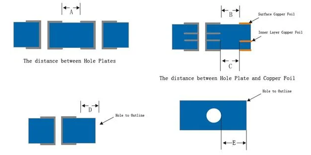
- IPC-2221: Generic standard suggesting minimum hole-to-hole spacing of 6 mils (0.15mm) for conventional boards
- IPC-7351: Addresses land pattern spacing including hole clearance
- Manufacturer Capabilities: Always consult your PCB fabricator’s design rules as they may have specific requirements based on their equipment
Typical minimum spacing guidelines:
| Feature Pair | Conventional PCB | HDI PCB |
|---|---|---|
| Via-to-via | 8 mil (0.2mm) | 6 mil (0.15mm) |
| Via-to-pad | 10 mil (0.25mm) | 8 mil (0.2mm) |
| Hole-to-edge | 15 mil (0.38mm) | 10 mil (0.25mm) |
| Drill-to-copper | 8 mil (0.2mm) | 6 mil (0.15mm) |
Note that these are general guidelines – high-reliability or high-voltage designs may require significantly greater spacing.
Best Practices for Proper Hole Spacing
1. Implement a Comprehensive Design Rule Check (DRC)
Configure your PCB design software’s DRC settings to include:
- Hole-to-hole spacing checks
- Hole-to-copper clearance verification
- Edge clearance monitoring
- Manufacturer-specific spacing rules
2. Consider Manufacturing Process Capabilities
Understand how your design choices affect fabrication:
- Mechanical Drilling: Requires larger spacing than laser drilling
- Stacked vs. Staggered Vias: HDI designs may need special spacing considerations
- Backdrilling Requirements: May necessitate additional spacing for depth control
3. Plan for Thermal and Mechanical Stress
- Increase spacing in areas subject to high thermal cycling
- Provide additional clearance around mounting holes
- Consider material properties when determining spacing in flexible circuits
4. Optimize for Assembly Processes
- Ensure adequate spacing for solder wave penetration
- Leave room for automated insertion equipment tolerances
- Account for press-fit connector installation forces
5. Use Advanced Design Techniques
- Apply via-in-pad technology carefully with proper spacing
- Implement teardrops where spacing is tight to strengthen connections
- Consider filled vias where spacing limitations exist
Case Studies: The Consequences of Ignoring Hole Spacing
Case 1: Consumer Electronics Failure
A smartphone design used tightly spaced microvias for processor breakout routing. While the design passed electrical verification, field failures showed cracked boards near the processor. Investigation revealed that thermal cycling caused stress fractures in the minimal material between vias. The solution involved redesigning with greater via spacing and using filled vias in critical areas.
Case 2: Industrial Control Board Rework
An industrial controller board experienced intermittent failures in humid environments. Testing found conductive anodic filament (CAF) growth between closely spaced plated through-holes. Increasing hole spacing and implementing additional conformal coating resolved the issue.
Case 3: Aerospace Application Rejection
A prototype avionics board failed qualification testing due to broken drill bits during fabrication. The designer had used the minimum spacing from a different manufacturer’s capabilities. Aligning the design with the actual fabricator’s requirements and adding 20% to their minimum spacing prevented the issue in the revised design.
Tools and Techniques for Managing Hole Spacing
Modern PCB design tools offer several features to help manage hole spacing:
- Interactive Spacing Guides: Real-time feedback during placement
- 3D Visualization: Identifying mechanical conflicts
- Manufacturing Rule Import: Loading fabricator-specific spacing requirements
- Automated Via Patterns: Generating properly spaced via arrays
- Cross-Section Analysis: Viewing spacing in the Z-axis for multilayer boards
Conclusion
Hole spacing in PCB design represents one of those subtle yet critical aspects that separate reliable, manufacturable boards from problematic ones. By giving proper attention to hole spacing considerations early in the design process, engineers can avoid costly re-spins, manufacturing delays, and field failures. The key lies in understanding the multifaceted impacts of hole spacing, implementing robust design rules, and maintaining clear communication with manufacturing partners.
As PCB technology continues advancing with finer features and higher densities, the importance of proper hole spacing only grows more pronounced. By making hole spacing a conscious priority rather than an afterthought, designers can significantly improve product quality while reducing time-to-market and manufacturing costs. In the complex ecosystem of PCB development, sometimes it’s the smallest spaces that make the biggest difference.