Rules setting before PCB routing
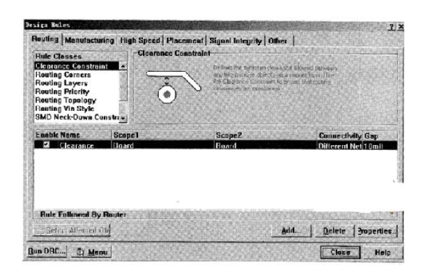
(1) Safety spacing setting
Setting the safety spacing corresponds to the Clearance Constraint item in Routing, which specifies the distance that must be maintained between the routing, pads, and vias of different networks on the board. The safety distance of a general PCB can be set to 0.254mm, a relatively empty board can be set to 0.3mm, and a denser patch board can be set to 0.2~0.22mm. The settings in PROTEL 995E are shown in Figure 1.
(2) Routing layer and direction setting
The routing layer and direction correspond to the Routing Layers item in Routing. Here you can set the routing layer used and the main routing direction of each layer. Please note that the single-sided board of the patch only uses the top layer, the single-sided board of the direct plug-in type only uses the bottom layer, but the power layer of the multi-layer board is not set here. The settings in PROTEL 99SE are shown in Figure 2.

(3) Setting of via shape
The via shape corresponds to the Routing Via Style item in Routing. It specifies the minimum, maximum and preferred values of the inner and outer diameters of the vias automatically generated during manual and automatic routing. The preferred value is the most important. The settings in PROTEL 995E are shown in Figure 3.

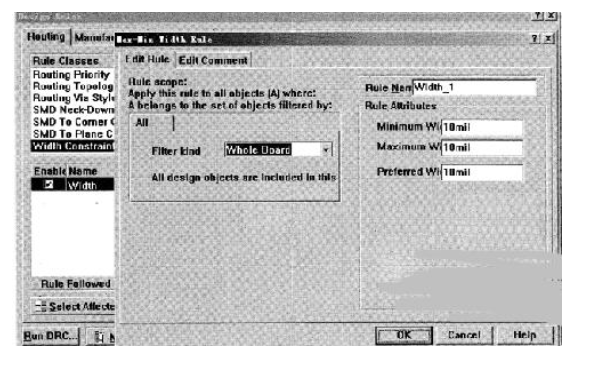
(4) Setting of trace width
The trace width corresponds to the Width Constraint item in Routing. It specifies the width of the trace during manual and automatic routing. The preferred option for the entire board range is 0.2 to 0.6 mm. In addition, the line width settings of some networks or network groups Net Class, such as ground wire power wire, AC power input wire, power output wire, power supply group, etc., can be defined in Design-NetlistManager in advance. The ground wire can generally be selected with a width of 1mm, and various power wires can generally be selected with a width of 0.5 to 1mm. The settings in PROTEL 995E are shown in Figure 4.