The Benefits of PCB Without Silkscreen: Why Going Bare Can Be Better
Introduction
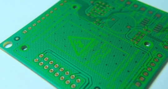
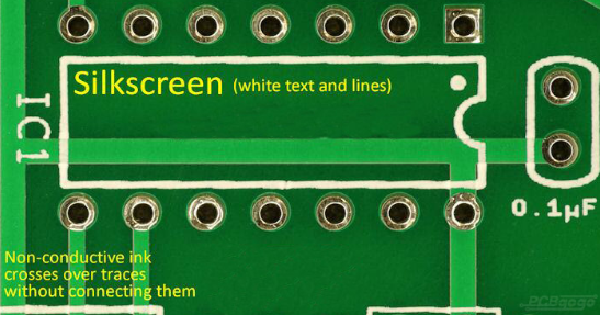
Printed Circuit Boards (PCBs) are the backbone of modern electronics, providing the necessary interconnections between components. Traditionally, PCBs include a silkscreen layer—a white (or sometimes other colored) ink layer that displays component outlines, reference designators, polarity markers, logos, and other essential information. However, as PCB technology advances, many designers are opting to eliminate the silkscreen altogether.
While silkscreen has its advantages, there are compelling reasons to design PCBs without it. This article explores the benefits of omitting the silkscreen layer, including cost savings, improved manufacturability, enhanced aesthetics, and better performance in high-frequency applications.
1. Cost Reduction
One of the most significant advantages of eliminating silkscreen is cost savings. The silkscreen process involves additional manufacturing steps, including:
- Ink Application: Silkscreening requires precise ink deposition, which adds time and complexity.
- Curing: The ink must be cured, increasing energy consumption and production time.
- Alignment: Accurate alignment is necessary to prevent misprinted markings, requiring extra quality control.
By removing silkscreen, manufacturers can streamline production, reduce material costs (ink), and minimize potential rework due to misprints. For high-volume production, these savings can be substantial.
2. Improved Manufacturability and Yield
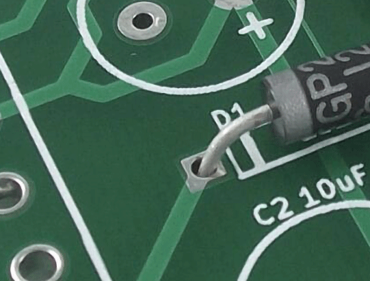
Silkscreen misalignment is a common issue in PCB manufacturing, particularly as board densities increase. When reference designators or polarity markers are misprinted, assembly errors can occur, leading to rework or even board failures.
- Tighter Tolerances: Modern PCBs, especially those with fine-pitch components, have little room for silkscreen inaccuracies.
- Laser-Direct Marking (LDM) Alternative: Instead of traditional silkscreen, some manufacturers use laser marking, which is more precise but also more expensive. Omitting silkscreen entirely avoids this trade-off.
- Fewer Defects: Without silkscreen, there is no risk of ink bleeding, smudging, or flaking over time.
For high-density interconnect (HDI) PCBs, where space is at a premium, eliminating silkscreen can improve assembly accuracy and reduce defects.
3. Enhanced Aesthetics and Minimalist Design
In consumer electronics and high-end devices, aesthetics play a crucial role. A PCB without silkscreen offers a cleaner, more professional appearance:
- Sleek Look: Without white (or colored) markings, the board appears more uniform, which can be desirable in transparent or open-design products.
- Minimalist Appeal: Many modern electronics favor a “no-label” design, where markings are either embedded in the solder mask or omitted entirely.
- Customization: Some designers prefer to use alternative labeling methods (engraved markings, hidden identifiers) for branding purposes.
4. Better Performance in High-Frequency Applications
For high-frequency and RF (radio frequency) PCBs, silkscreen ink can introduce unwanted effects:
- Dielectric Properties: Some silkscreen inks have dielectric characteristics that can slightly affect signal integrity at very high frequencies.
- Impedance Variations: In precision RF designs, even minor inconsistencies in the PCB surface (such as ink thickness) can impact impedance matching.
- Skin Effect Considerations: At microwave frequencies, current flows near the conductor’s surface, and any additional material (like silkscreen ink) can introduce losses.
By omitting silkscreen, designers ensure a more consistent substrate, reducing potential signal degradation.
5. Increased Durability and Reliability
Silkscreen ink is not as durable as the underlying PCB materials:
- Abrasion Resistance: Ink can wear off over time, especially in high-vibration or harsh environments.
- Chemical Exposure: Some cleaning agents or conformal coatings can degrade silkscreen markings.
- Long-Term Legibility: In critical applications (medical, aerospace), faded markings can lead to identification issues during maintenance.
Without silkscreen, the PCB relies on alternative identification methods (engraved labels, QR codes, embedded data), which are often more durable.
6. Simplified Design and Faster Turnaround
Removing silkscreen reduces design complexity:
- No Need for Silkscreen Layer in CAD: Designers can skip the step of placing reference designators and logos.
- Fewer Manufacturing Constraints: Without silkscreen, there’s no need to worry about minimum line widths, spacing, or ink coverage rules.
- Faster Prototyping: Some quick-turn PCB services offer faster production when silkscreen is omitted.
7. Better Suitability for Advanced Packaging Technologies
Emerging PCB technologies, such as:
- Embedded Components: Where passives or ICs are integrated into the substrate, silkscreen may not be practical.
- Flex and Rigid-Flex PCBs: Silkscreen can crack or peel on flexible sections.
- 3D-Printed Electronics: Additive manufacturing may not support traditional silkscreen processes.
In these cases, omitting silkscreen makes the design more compatible with cutting-edge fabrication techniques.
Conclusion
While silkscreen has been a standard feature of PCBs for decades, its elimination offers several advantages—cost savings, improved manufacturability, enhanced aesthetics, better high-frequency performance, increased durability, and design simplification. As PCB technology evolves, more designers may opt for “bare” boards, relying on alternative marking methods when necessary.
For applications where component identification is critical, solutions like laser marking, engraved labels, or digital documentation can replace traditional silkscreen without sacrificing functionality. Ultimately, the decision to exclude silkscreen depends on the specific requirements of the project, but its benefits make it a compelling option for modern PCB design.