High-speed circuit PCB design skills
(I) Introduction
The development and changes of electronic technology will inevitably bring many new problems and challenges to board-level design. First, due to the physical limits of high-density pins and pin sizes, low routing rate is caused; second, due to the increase in system clock frequency, timing and signal integrity problems are caused; third, engineers hope to use better tools on the PC platform to complete complex and high-performance designs. From this, it is not difficult to see that there are three trends in PCB board design:
The design of high-speed digital circuits (i.e. high clock frequency and fast edge rate) has become the mainstream.
Product miniaturization and high performance must face the distribution effect problem caused by mixed signal design technology (i.e. digital, analog and RF mixed design) on the same PCB board.
The increase in design difficulty has led to the traditional design process and design methods, as well as the CAD tools on the PC. It is difficult to cope with the current technical challenges. Therefore, the transfer of EDA software tool platforms from UNIX to NT platform has become a recognized trend in the industry.
(II) High-frequency circuit wiring skills
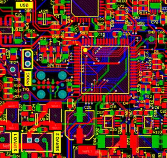
High-frequency circuits are often highly integrated and have a large wiring density. The use of multi-layer boards is both necessary for wiring and an effective means to reduce interference.
The fewer bends the lead wires between the pins of high-frequency circuit devices are, the better. It is best to use all-straight lines for the leads of high-frequency circuit wiring. If a turn is required, a 45° bend line or arc turn can be used. This requirement is only used to improve the adhesion strength of copper foil in low-frequency circuits, but in high-frequency circuits, meeting this requirement can reduce the external emission and mutual coupling of high-frequency signals.
The shorter the leads of high-frequency circuit device pins, the better.
The fewer alternations between the lead layers between high-frequency circuit device pins, the better. That is, the fewer vias (Via) used in the component connection process, the better. According to measurements, a via can bring about 0.5pF of distributed capacitance, and reducing the number of vias can significantly increase the speed.
When wiring high-frequency circuits, pay attention to the crosstalk introduced by the close parallel routing of signal lines. If parallel distribution cannot be avoided, a large area can be arranged on the reverse side of the parallel signal lines to greatly reduce interference. Parallel routing within the same layer is almost inevitable, but the directions of the routing on two adjacent layers must be perpendicular to each other.
Measures to surround particularly important signal lines or local units with ground wires should be implemented.
All kinds of signal lines should not form loops, and ground wires should not form current loops.
At least one high-frequency decoupling capacitor should be set near each integrated circuit block (IC), and the decoupling capacitor should be as close to the Vcc of the device as possible.
When analog ground wire (AGND) and digital ground wire (DGND) are connected to the common ground wire, a high-frequency choke should be used. When assembling the high-frequency choke link, a high-frequency ferrite bead with a wire in the center is often used. It can be treated as an inductor in the schematic diagram, and a component package is defined for it separately in the PCB component library. Before wiring, it is manually moved to a suitable position close to the common ground line.
(III) Electromagnetic compatibility (EMC) design method in PCB
The selection of PCB substrate and the setting of PCB layer number
the selection of electronic components and the electromagnetic characteristics of electronic components, component layout, the length and width of interconnection lines between components, etc. all restrict the electromagnetic compatibility of PCB. The integrated circuit chip (IC) on the PCB is the main energy source of electromagnetic interference (EMI). Conventional electromagnetic interference (EMI) control technology generally includes: reasonable layout of components, reasonable control of connections, reasonable configuration of power lines, grounding, filter capacitors, shielding and other measures to suppress electromagnetic interference (EMI) are very effective and widely used in engineering practice.

2.Wiring rules in electromagnetic compatibility (EMC) design of high-frequency digital circuit PCB
High-frequency digital signal lines should use short lines, generally less than 2 inches (5cm), and the shorter the better.
The main signal lines are best concentrated in the center of the PCB board.
The clock generation circuit should be near the center of the PCB board, and the clock fan-out should use daisy chain or parallel wiring.
The power line should be as far away from the high-frequency digital signal line as possible or separated by a ground line, and the distribution of the power supply must be low inductance (multi-channel design). The power layer in the multi-layer PCB is adjacent to the ground layer, which is equivalent to a capacitor and plays a filtering role. The power line and ground line on the same layer should also be as close as possible. The copper foil around the power layer should be indented 20 times the distance between the two plane layers than the ground layer to ensure that the system has better EMC performance. The ground plane should not be split. If the high-speed signal line is to be split across the power plane, several low-impedance bridge capacitors should be placed close to the signal line.
The wires used for input and output should be avoided as much as possible. It is best to add a ground wire between the wires to avoid feedback coupling.
When the copper foil thickness is 50um and the width is 1-1.5mm, the wire temperature is <3℃ when a current of 2A passes through. The wires of the PCB board should be as wide as possible. For integrated circuits, especially signal lines of digital circuits, a wire width of 4mil-12mil is usually selected. The power line and ground line should preferably have a wire width greater than 40mil. The minimum spacing of the wires is mainly determined by the insulation resistance and breakdown voltage between the wires in the worst case. Usually, a wire spacing of more than 4mil is selected. In order to reduce crosstalk between wires, the distance between the wires can be increased if necessary, and a ground wire can be inserted as a wire isolation.
In all layers of the PCB board, digital signals can only be routed in the digital part of the circuit board, and analog signals can only be routed in the analog part of the circuit board. The ground of the low-frequency circuit should be connected to the ground in parallel at a single point as much as possible. When the actual wiring is difficult, it can be partially connected in series and then connected to the ground in parallel. To realize the splitting of analog and digital power supply, the wiring cannot cross the gap between the split power supply. The signal line that must cross the gap between the split power supply should be located on the wiring layer next to the large area of ground.
There are two main electromagnetic compatibility problems caused by power supply and ground in PCB, one is power supply noise and the other is ground line noise. According to the size of the PCB board current, try to increase the width of the power line and reduce the loop resistance. At the same time, make the direction of the power line and ground line consistent with the direction of data transmission, which helps to enhance the anti-noise ability. At present, the noise of the power supply and ground plane can only be measured by the prototype product or by experienced engineers who set the capacity of the decoupling capacitor to the default value based on their experience.
2.Layout rules in electromagnetic compatibility (EMC) design of high-frequency digital circuit PCB
The layout of the circuit must reduce the current loop, shorten the connection between high-frequency components as much as possible, the distance between components susceptible to interference should not be too close, and the input and output components should be kept as far away as possible.
Arrange the positions of each functional circuit unit according to the flow of the circuit, so that the layout is convenient for signal flow and the signal keeps the same direction as much as possible.
Center on the core component of each functional circuit and lay it out around it. Components should be arranged evenly, neatly and compactly on the PCB, and the lead connections between components should be shortened as much as possible.
The PCB is divided into independent and reasonable analog circuit areas and digital circuit areas, and the A/D converter is placed across the partitions.
One of the common practices for PCB electromagnetic compatibility design is to configure appropriate decoupling capacitors at various key parts of the PCB board.
(IV) Signal Integrity (SI) Analysis
Signal Integrity (SI) refers to the quality of the signal on the signal line, which is the ability of the signal to respond with the correct timing and voltage in the circuit.
The high switching speed of integrated circuit chips (ICs) or logic devices, incorrect layout of terminal components or incorrect wiring of high-speed signals will cause signal integrity problems such as reflection, crosstalk, overshoot, undershoot, ringing, etc., which may cause the system to output incorrect data, the circuit to work abnormally or even not work at all.

Signal integrity and design of PCB
In the design of PCB, PCB designers need to integrate the layout and routing of components and the SI problem solution to be adopted in each case in order to better solve the signal integrity problem of PCB board. In some cases, the choice of IC can determine the number and severity of SI problems. Switching time or edge rate refers to the rate of IC state conversion. The faster the IC edge rate, the higher the possibility of SI problems. It is very important to terminate the device correctly.
A common method to reduce signal integrity problems in PCB design is to add termination components to the transmission line. In the termination process, the three requirements of the number of components, signal switching speed and circuit power consumption should be weighed. For example, adding termination components means that PCB designers have less space for routing, and it will be more difficult to add termination components in the later stage of layout processing because corresponding space must be reserved for new components and routing. Therefore, it should be clear whether termination components need to be placed in the early stage of PCB layout.


