What are the common methods of PCB anti-interference?
The anti-interference scheme of printed circuit boards is closely related to the specific circuit. Here we will only explain several common methods of PCB anti-interference scheme.
(1) Power line scheme
According to the size of the printed circuit board current, try to increase the width of the power line to reduce the loop resistance; at the same time, make the direction of the power line and ground line consistent with the direction of data transmission, which will help enhance the anti-noise ability.
(2) Ground line scheme
In the single-chip microcomputer system calculation, grounding is the primary method to control interference. If grounding and shielding can be used correctly, most interference problems can be solved. The ground line structure in the single-chip microcomputer system generally includes system ground, chassis ground (shield ground), digital ground (logic ground) and analog ground. The following points should be paid attention to in the ground line scheme:
① Correctly select single-point grounding and multi-point grounding.
In low-frequency circuits, the operating frequency of the signal is less than 1 MHz, and the inductance between its wiring and equipment has little effect, while the loop current formed by the grounding circuit has a greater impact on interference, so a single-point grounding method should be used. When the signal operating frequency is greater than 10 MHz, the ground impedance becomes very large. At this time, the ground impedance should be reduced as much as possible, and multi-point grounding should be used nearby. When the operating frequency is between 1 and 10 MHz, if a single-point grounding is used, the length of the ground wire should not exceed 1/20 of the wavelength, otherwise a multi-point grounding method should be used.
② Digital ground and analog ground are separated.
There are both high-speed logic circuits and linear circuits on the circuit board. They should be separated as much as possible, and the ground wires of the two should not be mixed, and they should be connected to the ground wire of the power supply end separately. The ground of the low-frequency circuit should be connected to the ground at a single point as much as possible. When the practical wiring is difficult, some can be connected in series and then connected in parallel; high-frequency circuits should use multi-point series grounding, and the ground wire should be short and thick. Use a large area of grid-shaped ground foil around high-frequency components as much as possible, and try to increase the grounding area of the linear circuit.
③ The grounding wire should be as thick as possible.
If the grounding wire is very thin, the grounding potential will change with the change of current, resulting in unstable timing signal level of electronic products and reduced anti-noise performance. Therefore, the grounding wire should be as thick as possible so that it can pass three times the allowable current of the printed circuit board. If possible, the width of the grounding wire should be greater than 3 mm.
④ The grounding wire forms a closed loop.
When designing a grounding system for a printed circuit board composed only of digital circuits, making the grounding wire a closed loop can significantly improve the anti-noise ability. The reason is that there are many integrated circuit components on the printed circuit board. Especially when there are components with high power consumption, due to the constraint of the thickness of the grounding wire, a large potential difference will occur on the grounding wire, resulting in reduced anti-noise ability; if the grounding wire forms a loop, the potential difference will be reduced, which will reduce the anti-noise ability of the electronic equipment.
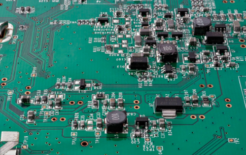
(3) Decoupling capacitor configuration
One of the common practices in PCB design is to configure appropriate decoupling capacitors at various key locations of the printed board. The general configuration principle of decoupling capacitors is:
① Connect a 10-100μF electrolytic capacitor across the power input terminal. If possible, it is better to connect more than 100μF.
② In principle, each integrated circuit chip should be equipped with a 0.01 pF ceramic capacitor. If the printed board is not spacious enough, a 1-10 pF tantalum capacitor can be arranged for every 4-8 chips.
③ For devices with weak anti-noise ability and large power supply changes when turned off, such as RAM and ROM storage devices, decoupling capacitors should be directly connected between the power line and ground line of the chip.
④ The capacitor lead should not be too long, especially the high-frequency bypass capacitor should not have leads.
In addition, the following two points should be noted:
① When there are touch devices, relays, buttons and other components in the printed board, large spark discharges will occur when they are operated, and it is necessary to use RC circuits to absorb the discharge current. Generally, R is 1-2 kΩ and C is 2.2-47μF.
② CMOS has a high input impedance and is easily induced. Therefore, when using it, the unnecessary end should be grounded or connected to the positive power supply.
(4) Oscillator
Almost all microcontrollers have an oscillator circuit coupled to an external crystal or ceramic resonator. On the PCB, the leads of the external capacitor, crystal or ceramic resonator should be as short as possible. The RC oscillator is potentially sensitive to interference signals and can produce a very short clock cycle. Therefore, the best choice is a crystal or ceramic resonator. In addition, the shell of the quartz crystal should be grounded.
(5) Lightning protection method
For microcontroller systems used outdoors or for power lines and signal lines that are overhead from outdoor to indoor, the lightning protection of the system should be considered. Commonly used lightning protection equipment includes: gas discharge tube, TVS (Transient Voltage Suppression), etc. When the power supply voltage of the gas discharge tube is greater than a certain value, generally tens of V or hundreds of V, the gas breaks down and discharges, and the strong impulse pulse on the power supply line is introduced into the ground. TVS can be regarded as two Zener diodes connected in parallel and in opposite directions, and it will conduct when the voltage at both ends is higher than a certain value. Its characteristic is that it can pass hundreds or even thousands of A of current in a transient state.
In order to improve the electromagnetic compatibility of the microcontroller system, it is necessary not only to reasonably design the PCB board, but also to adopt corresponding methods in the circuit structure and software. Practice shows that the electromagnetic compatibility of the microcontroller system needs to be considered at all stages of design, manufacturing, installation and operation. Only in this way can the system be ensured to operate stably, reliably and safely for a long time.