PCB Board Separation Stress Tester: A Comprehensive Guide
Abstract
The PCB (Printed Circuit Board) separation process is a critical step in electronics manufacturing, where stress-induced damage can significantly impact the reliability and performance of the final product. To mitigate these risks, PCB board separation stress testers are employed to measure and analyze the mechanical stresses exerted during the depaneling process. This article explores the principles, methodologies, applications, and benefits of PCB stress testing equipment, along with industry standards and future trends.
1. Introduction
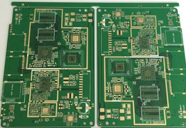
Modern electronics manufacturing relies heavily on PCBs, which often consist of multiple interconnected boards assembled in a panelized format for efficiency. Depaneling—the process of separating individual PCBs from the panel—can introduce mechanical stress, leading to microcracks, delamination, or component damage. To ensure product quality, manufacturers utilize PCB separation stress testers to quantify and optimize the depaneling process.
2. Understanding PCB Separation Stress
2.1 Sources of Stress During Depaneling
Several depaneling methods exist, including:
- V-Scoring & Breakout: Mechanical force applied to separate boards along pre-scored lines.
- Routing: Using a CNC router to cut PCBs from the panel.
- Laser Cutting: High-precision separation with minimal mechanical stress.
- Punching: Hydraulic or mechanical punching for high-volume production.
Each method induces different stress levels, which must be measured to prevent latent defects.
2.2 Impact of Excessive Stress
- Microcracks in Traces & Vias: Can lead to intermittent or complete electrical failures.
- Solder Joint Fractures: Weakens component connections, reducing product lifespan.
- Delamination: Separation of PCB layers, affecting structural integrity.
3. PCB Separation Stress Tester: Functionality & Design
3.1 Key Components
A typical PCB stress tester consists of:
- Force Sensors: Measure shear, tensile, and bending forces during separation.
- Data Acquisition System: Captures real-time stress data.
- Software Interface: Analyzes stress distribution and generates reports.
- Fixturing Mechanism: Secures the PCB panel for consistent testing.
3.2 Testing Methodologies
- Static Stress Testing: Measures constant force application (e.g., during punching).
- Dynamic Stress Testing: Evaluates stress variations during high-speed depaneling (e.g., routing).
- Thermal Stress Testing: Assesses combined mechanical and thermal effects (relevant for laser depaneling).
3.3 Industry Standards & Compliance
- IPC-6012: Defines acceptability criteria for rigid PCBs.
- IPC-A-600: Covers visual inspection standards.
- JEDEC JESD22-B104: Mechanical shock testing guidelines.
4. Applications of PCB Stress Testers
4.1 Process Optimization
By identifying excessive stress points, manufacturers can adjust:
- Cutting Speed & Feed Rate (for routers).
- Laser Power & Pulse Duration.
- Punching Force & Alignment.
4.2 Failure Analysis & Quality Control
Stress testers help:
- Detect weak PCB designs prone to cracking.
- Validate depaneling equipment settings.
- Ensure compliance with automotive/aerospace reliability standards.
4.3 R&D & New Material Testing
Evaluating stress resistance of:
- Flexible PCBs.
- High-Density Interconnect (HDI) Boards.
- Advanced Substrates (e.g., ceramic-filled laminates).
5. Benefits of Using PCB Stress Testers
- Improved Yield Rates: Reduces scrapped boards due to stress damage.
- Enhanced Product Reliability: Minimizes field failures.
- Cost Savings: Lowers warranty claims and rework expenses.
- Data-Driven Decisions: Enables process fine-tuning based on empirical data.
6. Future Trends in PCB Stress Testing
- AI-Powered Predictive Analytics: Machine learning models to predict stress-related failures.
- In-Line Real-Time Monitoring: Integration with smart manufacturing (Industry 4.0).
- Miniaturized Sensors: For testing ultra-thin and flexible PCBs.
- Automated Correction Systems: Immediate adjustment of depaneling parameters.
7. Conclusion
The PCB board separation stress tester is an indispensable tool in modern electronics manufacturing, ensuring that depaneling processes do not compromise product integrity. By leveraging advanced sensing technologies and data analytics, manufacturers can achieve higher yields, better reliability, and compliance with stringent industry standards. As PCB technology evolves, stress testing methodologies will continue to advance, integrating AI and automation for smarter, more efficient production.