PCB Trace Spacing: A Comprehensive Guide to Minimum Distance Between Conductors
Introduction to PCB Trace Spacing
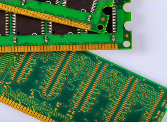
Printed Circuit Board (PCB) design involves numerous critical considerations, among which trace spacing remains one of the most fundamental yet complex aspects. The minimum distance between PCB traces, often referred to as “clearance” in the industry, affects everything from electrical performance to manufacturing yield and long-term reliability.
Trace spacing requirements have become increasingly stringent as electronic devices continue their relentless march toward miniaturization. Modern high-density interconnect (HDI) PCBs may contain thousands of traces packed into increasingly smaller areas, making proper spacing considerations more important than ever before.
This article will explore the multifaceted considerations surrounding PCB trace spacing, examining the electrical, manufacturing, and reliability factors that influence minimum distance requirements. We’ll cover industry standards, calculation methods, and practical design recommendations to help engineers create robust, high-performance PCB layouts.
Electrical Considerations for Trace Spacing
Voltage and Insulation Requirements
The primary electrical factor determining minimum trace spacing is the voltage difference between adjacent conductors. Higher voltage differences require greater spacing to prevent:
- Dielectric Breakdown: When the electric field strength exceeds the dielectric strength of the PCB material (typically FR-4), ionization can occur, leading to arcing or conductive paths forming between traces.
- Creepage and Clearance: Creepage refers to the shortest path between conductors along the surface of the insulation material, while clearance represents the shortest distance through air. Both must be considered for high-voltage applications.
Industry standards such as IPC-2221 provide tables and formulas for calculating minimum spacing based on voltage. For example:
- For 0-15V: 0.1mm minimum spacing
- For 16-30V: 0.1mm to 0.6mm depending on environment
- For 31-50V: 0.6mm minimum
- For 51-100V: 1.5mm minimum
These values increase significantly for higher voltages and harsh environments.
Signal Integrity and Crosstalk
Even in low-voltage digital circuits, trace spacing affects signal quality through:
- Crosstalk: Electromagnetic coupling between adjacent traces can cause unwanted signal transfer, especially at high frequencies. Crosstalk increases as spacing decreases and is affected by:
- Parallel run length
- Signal edge rates (rise/fall times)
- Dielectric material properties
- Reference plane placement
- Impedance Control: For controlled impedance traces, spacing affects coupling and therefore impedance values. Differential pairs, for instance, require precise spacing maintenance between the pair and other traces.
A general rule for digital signals is to maintain at least 3 times the dielectric thickness between traces carrying high-speed signals. For example, with a 0.2mm dielectric, maintain 0.6mm spacing for critical signals.
Manufacturing Constraints on Trace Spacing
PCB Fabrication Capabilities
While electrical requirements set the lower bound for trace spacing, manufacturing capabilities often determine what’s practically achievable:
- Standard PCB Manufacturers: Typically offer 0.1mm (4mil) minimum spacing
- Advanced/HDI Manufacturers: Can achieve 0.05mm (2mil) or less spacing
- Specialized RF/Microwave Shops: May offer 0.025mm (1mil) spacing with laser technology
These capabilities continue to improve, but designers must consider:
- Yield Impact: Tighter spacing reduces manufacturing yield and increases cost
- Registration Tolerance: Layer-to-layer alignment affects actual spacing in multilayer boards
- Etching Factors: Over-etching can reduce trace width, effectively increasing spacing
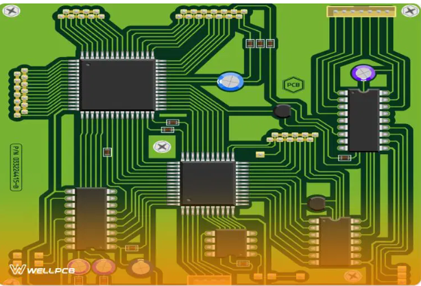
Design Rule Checks (DRC)
Modern PCB design software incorporates Design Rule Checking systems that enforce spacing constraints. Typical DRC settings include:
- Same Net Spacing: For different segments of the same net (e.g., between pads and traces)
- Different Net Spacing: Between unrelated conductors
- Component Spacing: Between component pads and traces
- Edge Clearance: Distance from board edges
Reliability and Environmental Factors
Long-Term Reliability Considerations
Proper trace spacing affects product lifespan through:
- Contamination: Dust, moisture, or ionic contamination can create leakage paths. Wider spacing improves reliability in harsh environments.
- Thermal Expansion: Different coefficients of thermal expansion can cause mechanical stress. Adequate spacing accommodates these movements.
- Electromigration: Over time, high current density can cause metal migration, especially with DC voltages and small spacings.
Environmental Classifications
IPC standards define three environmental classes that affect spacing requirements:
- Class 1 (General Electronics): Least stringent requirements
- Class 2 (Dedicated Service): Moderate requirements for longer life
- Class 3 (High Reliability): Most stringent for critical applications like aerospace or medical
For example, a 50V circuit might require:
- Class 1: 0.6mm spacing
- Class 2: 1.2mm spacing
- Class 3: 2.5mm spacing
Special Cases and Advanced Considerations
High-Frequency and RF Design
At microwave frequencies (above 1GHz), additional considerations apply:
- Skin Effect: Current concentrates at conductor surfaces, affecting loss and spacing requirements
- Surface Roughness: Impacts effective spacing at high frequencies
- Wave Coupling: Spacing affects propagation modes in transmission lines
Common RF spacing guidelines include:
- Maintain at least 3x dielectric thickness between traces
- Increase spacing for higher power levels
- Consider edge-coupled vs. broadside-coupled configurations
High-Current Applications
For power electronics, spacing must consider:
- Arc-over Potential: Higher currents can sustain arcs over greater distances
- Thermal Effects: Nearby heat sources affect insulation properties
- Fusing Considerations: Proper spacing prevents collateral damage during faults
Mixed-Signal Design
When analog and digital circuits coexist:
- Ground Plane Separation: Often requires increased spacing between analog and digital sections
- Noise-Sensitive Signals: May need guard traces with specific spacing
- Power Supply Isolation: Switching regulators require careful spacing of noisy traces
Practical Design Recommendations
General Spacing Guidelines
For typical FR-4 boards with 1oz copper:
- Low-Voltage Digital (≤15V): 0.15mm minimum, 0.2mm recommended
- Medium Voltage (16-30V): 0.3mm minimum, 0.5mm recommended
- High Voltage (≥50V): Follow IPC-2221 tables based on environmental class
- High-Speed Digital: 3x dielectric thickness between critical signals
- Power Traces: At least 1mm spacing for typical power levels
Calculation Methods
For precise calculations:
- IPC-2221 Formulas:
- Internal layers: Spacing = (Voltage + 25) / 25 (mm)
- External layers: Spacing = (Voltage + 50) / 50 (mm)
(With environmental multipliers)
- Peak Voltage Considerations: Account for transients and ringing
- Altitude Derating: Above 3000m, increase spacing by 5% per 300m
Design for Manufacturing (DFM)
To ensure manufacturability:
- Consult Your Fabricator: Get their specific capabilities
- Add Margin: Design slightly above minimum specs
- Consider Panelization: Spacing affects routing and scoring
- Test Structures: Include spacing test coupons for verification
Future Trends in PCB Trace Spacing
As technology advances, several trends are emerging:
- Advanced Materials: New substrates with higher dielectric strength enabling tighter spacing
- Embedded Components: Moving passives inside the board affects spacing requirements
- 3D Printing: Additive manufacturing may redefine spacing limitations
- Molecular Electronics: Ultimately approaching atomic-scale spacing
However, fundamental physics constraints will always play a role in determining minimum practical spacing.
Conclusion
PCB trace spacing represents a critical balance between electrical requirements, manufacturing capabilities, and reliability considerations. While modern technology allows for increasingly dense layouts, designers must carefully evaluate all factors when determining appropriate conductor spacing.
By understanding the underlying principles, applying relevant standards, and collaborating with fabrication partners, engineers can develop PCB layouts that are both high-performance and manufacturable. The key lies in recognizing that minimum spacing isn’t just about what’s possible, but what’s optimal for the specific application and its requirements.
As electronic systems continue their relentless progression toward higher density and higher performance, the importance of proper trace spacing will only grow more pronounced. Mastering this fundamental aspect of PCB design remains essential for creating reliable, high-quality electronic products.