How to systematically learn PCB design
With the accelerated rise of smart hardware, circuit boards are an indispensable part of many products. The current period is the blowout period of the circuit board industry, and the profession of PCB development engineer is very popular in China. If you want to become a high-paid engineer, you must fully master the professional skills and knowledge of PCB.
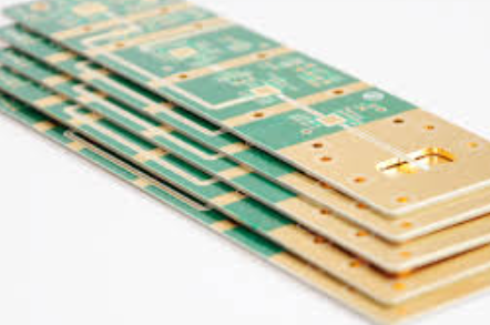
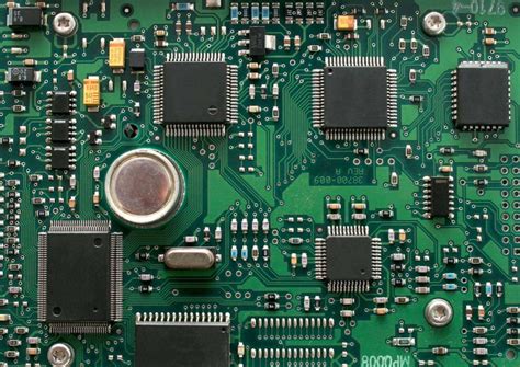
So what is PCB? The Chinese name of PCB is printed circuit board, also known as printed circuit board, printed circuit board, which is an important electronic component, a support for electronic components, and a provider of electrical connections for electronic components. Because it is made by electronic printing, it is called a “printed” circuit board. As the PCB size requirements become smaller and smaller, the device density requirements become higher and higher, and the difficulty of PCB design becomes greater and greater.
How to achieve a high PCB routing rate and shorten the design time? Here is a brief talk about the design skills of PCB planning, layout and wiring.
Determine the number of layers of PCB
The size of the circuit board and the number of wiring layers need to be determined in the early stage of design. The number of wiring layers and the stack-up method will directly affect the wiring and impedance of the printed line. The size of the board helps to determine the stacking method and the width of the printed line to achieve the desired design effect. At present, the cost difference between multilayer boards is very small. It is best to use more circuit layers and evenly distribute the copper when starting the design.
Design rules and restrictions
To successfully complete the wiring task, the wiring tool needs to work under the correct rules and restrictions. To classify all signal lines with special requirements, each signal class should have a priority. The higher the priority, the stricter the rules. The rules involve the width of the printed line, the maximum number of vias, parallelism, the mutual influence between signal lines, and the restrictions of the layer. These rules have a great impact on the performance of the wiring tool.
Component layout
During the optimization assembly process, the design for manufacturability (DFM) rules will restrict the layout of components. If the assembly department allows the movement of components, the circuit can be properly optimized to facilitate automatic wiring. The defined rules and constraints will affect the layout design. The automatic wiring tool will only consider one signal at a time. By setting the constraints for wiring and setting the layers where the signal lines can be laid, the wiring tool can complete the wiring as the designer envisions.
How to layout the power line:
①
In the PCB layout, the power decoupling circuit should be designed near the relevant circuits, rather than placed in the power supply part, otherwise it will affect the bypass effect and cause pulsating current to flow through the power line and ground line, causing interference.
②
For the power supply direction inside the circuit, the power supply should be supplied from the final stage to the front stage, and the power filter capacitor of this part should be arranged near the final stage.
③
For some major current channels, such as disconnecting or measuring current during debugging and testing, current gaps should be arranged on the printed conductors during layout.
In addition, it should be noted that the voltage-stabilized power supply should be arranged on a separate printed circuit board as much as possible during layout. When the power supply and circuit share the printed circuit board, in the layout, the voltage-stabilized power supply and circuit components should be mixed or the power supply and circuit should be shared with the ground line. Because this kind of wiring is not only prone to interference, but also the load cannot be disconnected during maintenance, and only part of the printed conductor can be cut, thereby damaging the printed circuit board.
Component layout
Most materials mention that capacitors should be placed as close to the chip as possible. Most materials discuss this placement distance issue from the perspective of reducing loop inductance. But there is another important reason, which is the capacitor decoupling radius issue.
The best way to understand the decoupling radius is to examine the phase relationship between the noise source and the capacitor compensation current. When the chip’s demand for current changes, a voltage disturbance will be generated in a very small local area of the power plane. To compensate for this current (or voltage), the capacitor must first sense this voltage disturbance.
When the distance from the disturbance area to the capacitor is reached, the decoupling effect fails and the compensation energy cannot be delivered in time. In order to effectively transmit the compensation energy, the phase difference between the noise source and the compensation current should be as small as possible, preferably in the same phase.
For example: If the total parasitic inductance of a 0.001uF ceramic capacitor is 1.6nH after being installed on the circuit board, then its resonant frequency after installation is 125.8MHz and the resonant period is 7.95ps. Assuming that the signal propagates at a speed of 166ps/inch on the circuit board, the wavelength is 47.9 inches. The decoupling radius of the capacitor is 47.9/50=0.958 inches, which is approximately equal to 2.4 centimeters.
The capacitor in this example can only compensate for the power supply noise within a range of 2.4 centimeters around it, that is, its decoupling radius is 2.4 centimeters. Different capacitors have different resonant frequencies and different decoupling radii. For large capacitors, because their resonant frequencies are very low, the corresponding wavelengths are very long, so the decoupling radius is very large, which is why we don’t pay much attention to the placement of large capacitors on the circuit board. For small capacitors, because the decoupling radius is very small, they should be as close to the chip that needs to be decoupled as possible. This is exactly what most materials will repeatedly emphasize, and small capacitors should be placed as close to the chip as possible.
There will also be impatient engineers who can’t wait to put the devices in place and start pulling wires after drawing the schematic and importing the netlist into the PCB. In fact, a good PCB layout can make your subsequent pulling work simple. Each board will have a signal path, and the PCB layout should also try to follow this signal path so that the signal can be transmitted smoothly on the board. If the schematic is designed according to the module, the PCB can also be the same.
Therefore, there are more stringent and more professional skill requirements for PCB designers. However, the current situation of most PCB engineers is limited to the PCB design of some simple or single products.