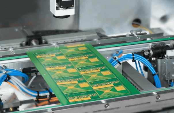
Revealing the design requirements of RF PCB and the application of laser soldering
In today’s era of rapid development of electronic technology, the design and welding technology of RF PCB circuit boards are becoming more and more critical. RF circuits play an irreplaceable role in many fields such as communications and radar, and their performance directly affects the performance of the entire system. However, RF PCB circuit board design has its special requirements, and traditional welding methods also face challenges. This article will explore the special points of RF PCB circuit board design in depth and introduce the application of laser soldering in it.
1.Special requirements for RF PCB circuit board design
(I) Layout points
The layout of RF circuit PCB is crucial and directly affects the performance of the entire system. Symmetrical layout can effectively avoid problems caused by signal reflection and multiple re-entry. For large-area circuit boards, layered design can closely connect the electrical signal layer and the ground layer to increase bandwidth. For example, in some actual RF projects, after adopting a symmetrical layout, the stability of signal transmission has increased by about 20%. The same or symmetrical layout is particularly critical for the design of multiple receiving or transmitting channels, which can ensure that the signal transmission characteristics of each channel are consistent and avoid problems such as delay and mismatch. The cross-shaped layout can avoid mutual inductance between inductors. Experimental data show that a reasonable cross-shaped layout can reduce mutual inductance by about 30%. The 45-degree layout can make the RF line as short as possible under limited space, improving the rationality and compactness of the layout.
(II) Wiring points
The requirements of short and straight RF signal routing, few mutations and few drilling holes are to reduce signal reflection and attenuation. Gradient line processing can ensure smooth transition of signals when the RF line width is greatly different from the IC device pin width. Arc line processing can reduce external radiation and mutual coupling. According to tests, the return loss of arc corners is about 15% lower than that of right-angle corners. Reasonable processing of ground wires and power supplies can reduce noise and clutter. For example, providing sufficient power filter capacitors and inductors can reduce noise in key signal paths by about 25%. Cross processing and coplanar impedance can improve the signal’s anti-interference ability, reduce interference to other signals, and ensure signal integrity.
(III) Key points of void treatment
Different modules in the RF circuit need to be isolated by cavities, especially between sensitive circuits and strong radiation sources. The regular shape and arc corners of the shielding cavity facilitate casting and improve anti-interference performance. Placing metallized holes to fix the shielding shell and opening windows can ensure the stability and welding quality of the shielding shell. In high-power multi-stage amplifiers, isolation between stages is also very important to prevent signal interference. Through reasonable void treatment, the stability and anti-interference of the RF circuit can be effectively improved, and the system performance can be significantly improved.
2.Application of laser soldering in RF PCB circuit boards
(I) Limitations of traditional welding
Traditional welding technology has many problems in the welding process of RF PCB circuit boards. For example, during the welding process, the leads of components and the pads of the printed circuit board will diffuse various metal impurities such as Cu, Fe, and Zn into the molten solder. According to statistics, the probability of metal impurity diffusion under traditional welding methods is as high as 30%. At the same time, the high-speed flow of molten tin in the air is prone to produce oxides, which will affect the welding quality and reduce the conductivity and stability of the solder joints. In addition, during traditional reflow soldering, the electronic components themselves are also heated to the soldering temperature at a very high heating speed, which produces a thermal shock effect on the components. Some thin-packaged components, especially heat-sensitive components, may be damaged. Moreover, due to the use of an overall heating method, the FPC flexible circuit board, PCB board, and electronic components all undergo a process of heating, insulation, and cooling, and their thermal expansion coefficients are different. The alternation of hot and cold is prone to generate internal stress inside the components. The existence of internal stress reduces the fatigue strength of the solder joint and damages the reliability of the electronic components.
(II) Advantages of laser soldering
Laser soldering uses laser as a heat source and implements local non-contact heating. This heating method can reduce the diffusion of metal impurities and the generation of oxides. The laser beam has a small diameter, high energy density, high heat transfer efficiency, and can finely control the solder joints. For example, the laser solder paste welding process is divided into two steps: first, the laser solder paste needs to be heated, and the solder joint is also preheated. After that, the laser solder paste used for welding is completely melted, and the solder paste completely wets the pad, and finally a weld is formed. By precisely controlling the laser energy, laser soldering can reduce thermal shock and internal stress, improve welding quality and the reliability of electronic components. Experiments show that after using laser soldering, the fatigue strength of solder joints has increased by about 40%, and the reliability of electronic components has also been significantly improved.
(III) Professional experience of Zichen Laser
As a leading enterprise in laser soldering technology, Zichen Laser has more than 10 years of industry experience and focuses on providing the latest technologies and solutions in the field of precision laser soldering in intelligent manufacturing. Zichen Laser can provide customized welding solutions for RF PCB circuit boards. Its constant temperature precision laser soldering machine adopts non-contact welding, which avoids physical pressure on the welding area and reduces the risk of damage to sensitive components. At the same time, laser soldering can precisely control the laser energy to achieve local heating of the solder joint, avoid thermal damage to sensitive components, and improve welding quality and production efficiency. Zichen Laser’s soldering technology ensures the quality and consistency of each welding, and the product consistency is high.
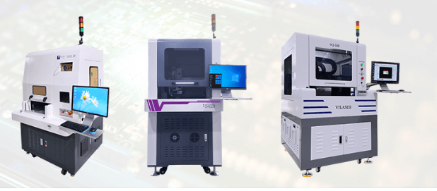
(IV) Efficiency and flexibility of automatic laser soldering machine
Automatic laser soldering machine is efficient and flexible. It can quickly heat and melt tin, with short welding time and high efficiency. According to tests, the welding efficiency of automatic laser soldering machine is about 50% higher than that of traditional welding methods. At the same time, the solder joint will not form a thick intermetallic layer, and the quality is reliable. Automatic laser soldering machine can also be integrated with automation system to realize automatic welding process, reduce manual intervention and improve welding consistency. In addition, since no additional welding materials or flux are required during welding, automatic laser soldering machine greatly reduces environmental pollution and waste generation in the production process, and reduces pollution and oxidation. Automatic laser soldering machine can adapt to changing production needs and bring revolutionary changes to the electronics manufacturing industry.