High-Speed Digital PCB Design Considerations
Abstract
This paper explores the critical considerations in designing printed circuit boards (PCBs) for high-speed digital circuits. As digital systems continue to operate at higher frequencies with faster edge rates, traditional PCB design approaches become inadequate. This article examines signal integrity, power integrity, electromagnetic compatibility, material selection, and layout techniques essential for successful high-speed digital PCB design. Practical design guidelines and mitigation strategies are provided to address common challenges in high-speed digital implementations.
1. Introduction
The proliferation of high-performance computing, 5G communications, and advanced digital interfaces has pushed digital circuit speeds into the multi-gigahertz range. Modern digital systems with clock frequencies exceeding 1 GHz and edge rates below 100 ps have made PCB design significantly more challenging. At these speeds, PCB traces no longer behave as simple conductors but as transmission lines where signal integrity considerations dominate the design process.
Successful high-speed digital PCB design requires careful attention to several interrelated factors: controlled impedance routing, proper termination strategies, power distribution network design, electromagnetic interference (EMI) control, and careful material selection. This paper systematically addresses these considerations to provide designers with a comprehensive framework for high-speed digital PCB implementation.
2. Signal Integrity Fundamentals
2.1 Transmission Line Theory
At high frequencies, PCB traces exhibit transmission line behavior where the propagation delay becomes comparable to the signal rise time. When the trace length exceeds approximately 1/6 of the signal’s rising edge wavelength, transmission line effects must be considered. The critical length can be calculated as:
Lcritical = (tr × v) / 6Where:
- tr = signal rise time
- v = signal propagation velocity (~6 in/ns for FR4)
For a 100 ps rise time, traces longer than about 1 inch require transmission line treatment.
2.2 Characteristic Impedance
Maintaining consistent characteristic impedance is essential for minimizing reflections. Microstrip and stripline are the two primary configurations:
Microstrip (surface trace):
Z0 ≈ (87/√(εr + 1.41)) × ln(5.98h/(0.8w + t))Stripline (embedded trace):
Z0 ≈ (60/√εr) × ln(4h/(0.67π(0.8w + t)))Where:
- Z0 = characteristic impedance (Ω)
- εr = dielectric constant
- h = dielectric height
- w = trace width
- t = trace thickness
Typical values range from 50Ω to 75Ω for single-ended signals and 90Ω to 100Ω for differential pairs.
2.3 Termination Strategies
Proper termination prevents signal reflections that can cause overshoot, undershoot, and ringing. Common techniques include:
- Series Termination: A resistor at the driver matching Z0 – driver impedance
- Parallel Termination: A resistor at the receiver matching Z0 to ground
- Thevenin Termination: Voltage divider network at receiver
- AC Termination: Capacitor in series with parallel termination
3. Power Integrity Considerations
3.1 Power Distribution Network (PDN)
A low-impedance power delivery system is critical for high-speed designs. Key aspects include:
- Decoupling Capacitor Strategy: Use multiple capacitor values (bulk, ceramic, high-frequency) placed close to IC power pins
- Power Plane Design: Prefer solid planes over split planes when possible
- Impedance Target: Typically < 1Ω across the relevant frequency spectrum
3.2 Simultaneous Switching Noise (SSN)
When multiple outputs switch simultaneously, the resulting current surges can cause ground bounce and power droop. Mitigation techniques include:
- Distributing ground connections evenly
- Using multiple vias for power and ground connections
- Implementing proper decoupling strategies
- Staggering output switching when possible
4. Electromagnetic Compatibility (EMC)
4.1 Radiated Emissions
High-speed signals can act as unintentional antennas. Control methods include:
- Proper termination to reduce harmonic content
- Careful routing to minimize loop areas
- Use of ground planes as shields
- Strategic placement of filter components
4.2 Crosstalk Reduction
Unwanted coupling between signals can be minimized by:
- Maintaining 3× trace width spacing between critical traces
- Routing sensitive signals on different layers with ground shielding
- Using orthogonal routing on adjacent layers
- Implementing guard traces with grounded vias for critical signals
5. Material Selection
5.1 Dielectric Materials
FR4 is common but may not be suitable for very high-speed designs (>5 GHz). Alternative materials with better performance include:
- Rogers RO4000 series (εr ≈ 3.3-3.5)
- Isola I-speed (εr ≈ 3.7)
- Nelco N4000-13 (εr ≈ 3.4)
Key parameters to consider:
- Dielectric constant (εr) consistency
- Loss tangent (dissipation factor)
- Thermal stability
- Moisture absorption
5.2 Copper Foil Characteristics
The copper surface roughness affects signal loss at high frequencies:
- Standard ED (Electrodeposited) copper: higher roughness
- RTF (Reverse Treat Foil): smoother surface
- HVLP (Hyper Very Low Profile): lowest roughness
6. Layout Techniques
6.1 Layer Stackup Design
A well-planned stackup provides controlled impedance and reduces EMI. A typical 8-layer stackup might be:
- Signal (microstrip)
- Ground plane
- Signal (stripline)
- Power plane
- Ground plane
- Signal (stripline)
- Power plane
- Signal (microstrip)
6.2 Routing Practices
- Maintain consistent trace widths within a net
- Minimize use of vias for high-speed signals
- Avoid 90° angles (use 45° or curved traces)
- Route differential pairs with tight coupling
- Match trace lengths for timing-critical signals
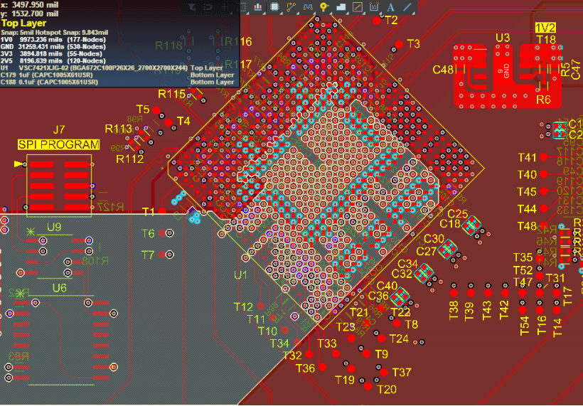
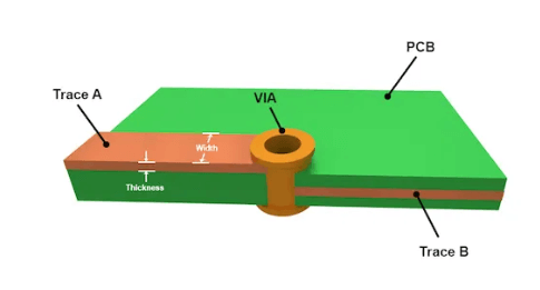
6.3 Via Design
Vias introduce discontinuities that can affect signal integrity:
- Use smaller diameter vias for higher frequencies
- Implement via stitching for ground connections
- Consider back-drilling for removing unused via stubs
- Use via-in-pad with fill for dense BGA routing
7. Design Verification
7.1 Simulation Tools
Modern EDA tools provide essential simulation capabilities:
- SPICE-based circuit simulation
- 2D and 3D electromagnetic field solvers
- Power integrity analysis
- Signal integrity analysis (eye diagrams, TDR)
7.2 Measurement Techniques
Physical verification methods include:
- Time Domain Reflectometry (TDR)
- Vector Network Analyzer (VNA) measurements
- Near-field EMI scanning
- Power rail measurements with high-bandwidth probes
8. Future Trends
Emerging challenges in high-speed PCB design include:
- Designs supporting 112Gbps and beyond SERDES
- Increased integration of optical interconnects
- Advanced packaging techniques (2.5D/3D IC)
- AI-assisted layout optimization
- Sustainable material development
9. Conclusion
High-speed digital PCB design requires a holistic approach that balances signal integrity, power integrity, and electromagnetic compatibility requirements. By understanding transmission line behavior, implementing proper termination strategies, designing robust power delivery networks, and selecting appropriate materials, designers can successfully implement reliable high-speed digital systems. As data rates continue to increase, these considerations will become even more critical for successful product development.
The guidelines presented in this paper provide a foundation for addressing the complex challenges of high-speed digital PCB design. However, each design presents unique requirements, and designers must apply these principles judiciously while considering the specific constraints of their application. Continuous learning and adaptation to new technologies will remain essential as digital systems push performance boundaries.