How to make trade-offs in the design of PCB power distribution network
When designing a more complex board, you must make some design trade-offs. Because of these trade-offs, there are some factors that affect the design of PCB power distribution network.
When the capacitor is installed on the PCB, there will be an additional loop inductance, which is related to the installation of the capacitor. The size of the loop inductance value depends on the design. The size of the loop inductance depends on the line width and line length of the line from the capacitor to the via, the length of the trace (i.e. the length of the plane connecting the capacitor and the power/ground plane), the distance between the two holes, the diameter of the hole, the pad of the capacitor, and so on. As shown in Figure 1, the installation diagrams of various capacitors.
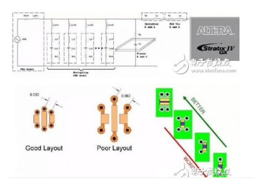
Figure 1 The best and worst capacitor layout
Design points to reduce capacitor loop inductance:
■The hole should be placed as close to the capacitor as possible. Reduce the distance between the power/ground holes. If possible, use multiple pairs of power/ground holes in parallel. For example, two holes with opposite current polarity should be placed as close as possible, and holes with the same current polarity should be placed as far as possible.
■ Use short, wide traces to connect vias to capacitor pins.
■ Place capacitors on the PCB surface (top and bottom layers) as close to their corresponding power/ground planes as possible. This minimizes the distance between vias. Use thin dielectrics between power/ground.
Next are three different design scenarios for capacitor mounting and propagation inductance. Figure 2 shows how various design scenarios introduce loop inductance.
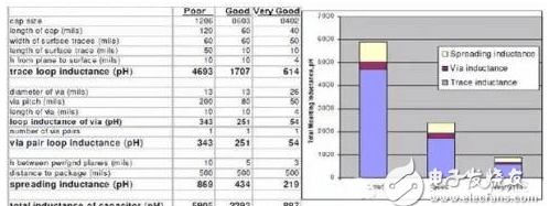
Figure 2 Design scenarios
Scenario 1 – Poor design
■ The designer does not pay attention to the design of the power distribution network (PDN).
■ The spacing between vias is not optimized.
■ The distance between power and ground planes is not optimized.
■ The trace distance from vias to capacitor pins is long.
For the total loop inductance, the loop inductance mainly comes from the routing, because the trace length in the poor design is 5 times longer than in the other two scenarios (good design and very good design). The distance from the bottom layer where the capacitor is mounted to the nearest plane is also a major factor in the loop inductance. Because this is not optimized (10mil), the routing has a significant impact on the overall loop inductance. Also, because the designer used 10mil dielectric material between power and ground, the secondary contributor to the loop inductance is the propagation inductance. The effect of not optimizing the distance between vias is not as significant as the length of the vias. The effect of the vias becomes larger for longer vias.
Case 2 – Good Design
■ The designer paid attention to the design of some power distribution networks (PDNs).
■ The spacing of the vias was improved. The length of the vias remained the same.
■ The distance between the power and ground planes was improved.
■ The routing distance from the vias to the capacitor pins was optimized.
The loop inductance of the routing is still the main contributor to the overall loop inductance. However, the routing loop inductance of the good design is about 2.7 times smaller than the routing loop inductance of the poor design. Because the designer reduced the thickness of the dielectric from 10mil to 5mil, the propagation inductance was reduced by half. The effect of the vias was slightly improved due to the reduced distance between the vias.
Case 3 – Very Good Design
■ The designer paid great attention to the design of the PDN.
■ The hole spacing and length are improved.
■ The distance between power and ground is also fully optimized.
■ The trace distance from the via to the capacitor pin is optimized.
The trace inductance of the very good design is about 7.65 times smaller than the trace inductance of the poor design. This is achieved by reducing the trace length and reducing the thickness of the bottom surface where the capacitor is mounted to the nearest plane layer on the PCB. Since the designer has optimized the dielectric layer thickness between the power and ground, the propagation inductance is greatly reduced. The loop inductance of the via is also significantly improved because the hole spacing and hole length are greatly reduced. Compared to the poor design, the total loop inductance of the very good design case is reduced by reducing one of the seven major factors. .
In the PCB board, additional via loop inductance is introduced by mounting the capacitor, which reduces the resonant frequency of the capacitor. This factor must be considered when designing your power distribution network (PDN). When designing at high frequencies, reducing loop inductance is the only visible way to reduce impedance.
For a given power supply, the report generated by the PDN tool shows that the PCB cutoff frequency is higher for the very good design compared to the very bad design. This may be the opposite of the expected result, because more capacitors are required to decouple the higher cutoff frequency than to decouple the lower cutoff frequency.
For the very good design case, the higher cutoff frequency means that the higher frequency can be decoupled. The capacitors placed on the PCB board have a decoupling effect on noise up to a higher frequency.
For the bad design case, the PCB board cannot be decoupled above the lower cutoff frequency. Any additional capacitance, that is, adding decoupling capacitors above the cutoff frequency, only increases the BOM cost without any effect on the decoupling effect. For the bad design case, the design of the power distribution network is more susceptible to noise at a certain frequency than the very good design.
As another example, suppose a 20-layer PCB board has a total thickness of 115mil. The power layer is on layer 3. The thickness from layer 1 (the layer where the FPGA is located) to layer 3 is 12mil. Then the thickness from the bottom layer to the third layer is 103mil. The power and ground layers are separated by a 3mil dielectric. The inductance of the BGA hole for this track is 5nH (5 pairs of holes for this power track). In order to cope with the relatively dense layout and routing area on the first layer, the associated decoupling capacitors are installed on the bottom layer. Since this installation will have long vias, this trade-off design leads to a high capacitor installation inductance value. After full optimization, the installation inductance of the 0402 package capacitor on the bottom layer is 2.3nH, while the installation inductance of the same capacitor on the first layer is 0.57nH.
To improve the PDN effect of this track, you can place some high-frequency capacitors on the first layer, while keeping the mid-frequency and bulk capacitors in their original positions, that is, on the bottom layer. This circuit design is a cut-off solution for PDN because high-frequency capacitors are the first response capacitors below the cut-off frequency. The effect of the capacitor depends on the total loop inductance (capacitor installation inductance + propagation inductance + BGA hole inductance) and the FPGA. You can place the high-frequency capacitor on the first layer and a little away from the FPGA. The propagation inductance of the capacitor placed outside the FPGA breakout area is 0.2nH. This new placement method is beneficial compared to the original method of placing it on the bottom layer because the total loop inductance (0.57nH+0.2nH+0.05nH=0.82nH) is less than the total inductance when placed on the bottom layer.
The propagation inductance of the PCB board is design-dependent and exists uniformly in the dielectric between the power and ground planes. 3mil thickness or thinner is the best design to reduce the plane propagation inductance. You can improve the performance of the PDN by following the design guidelines below.
The following are design guidelines about the importance of order, from the first layer to the bottom layer—the design guidelines on the first layer are the most important.
■ Reduce the dielectric thickness between the power and ground layers. When designing the board stackup, determine the power, layer, and other layers. For example, a stackup of PWR1 – GND1 – SIG1 – SIG2- GND2 – PWR2 is better than a stackup of PWR1 – SIG1 – GND1 – SIG2 – GND2 – PWR2. The second case results from a design that does not optimize the distance between power and ground. This setup results in a large capacitor propagating more inductance between PWR1/GND1 than between PWR2/GND2. You can find a typical dielectric thickness of 3 mils between the power and ground planes without adding extra cost. For additional performance improvement, consider a dielectric thickness thinner than 3 mils. However, this will increase the cost of the PCB.
■ When selecting capacitors, select multiple capacitor values instead of selecting a large capacitor of the same value to achieve the target impedance. In a PDN, the peak of the impedance is formed by a resonant reaction. A high ESR at the resonant frequency can suppress the resonance, thereby reducing the height of the impedance peak. Using a few capacitors of the same capacitance value at the capacitor’s resonant frequency and the impedance peak can effectively reduce the ESR.
A wide range of frequencies can maintain a relatively high ESR by selecting capacitors with multiple capacitance values.
■ Choose the location of high-frequency capacitors to reduce the total loop inductance. The total inductance is composed of the capacitor’s ESL, mounting inductance, propagation inductance, and BGA via inductance. When placing capacitors, place high-frequency capacitors first, followed by mid-frequency and low-frequency capacitors.
■ When splitting the plane, make sure the plane is properly square. Avoid narrow plane shapes, as this will limit the current and increase the plane’s propagation inductance.
■ Mid-frequency and low-frequency capacitors are not as sensitive to how they are placed. They can be placed slightly away from the FPGA.
Weighing the situation of multi-channel design
On a PCB with multiple peripherals, your design can no longer share a power supply. This may require you to implement DDR power interfaces through your design, combine power traces of various I/O ports, or combine power traces of various receivers to reduce PCB BOM cost and PCB layout complexity.
Power trace sharing increases the complexity of the PDN and also adds a lot of noise on the PCB and at the die location. For multi-channel situations, there are two main steps to design a power distribution solution:
1 Low frequency solution
2 High frequency solution
At very low frequencies, the first step is to ensure that the size of the VRM is suitable for handling various current needs.