Understanding PCB Return Current: How It Is Generated and the Role of Return Paths
Introduction
Printed Circuit Boards (PCBs) are fundamental components in modern electronics, enabling the interconnection of various electrical and electronic components. A critical aspect of PCB design is managing current flow, particularly the return current, which plays a vital role in signal integrity, electromagnetic compatibility (EMC), and overall circuit performance.
This article explores how PCB return current is generated, the importance of return paths, and how proper design techniques can mitigate issues such as noise, crosstalk, and electromagnetic interference (EMI).
1. How PCB Return Current Is Generated
1.1 Basic Principles of Current Flow
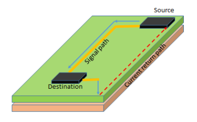
In any electrical circuit, current flows in a closed loop. When a signal is transmitted from a source to a load (e.g., a microcontroller to an IC), the current must return to its origin to complete the circuit. This return path is often through a ground plane, a power plane, or a dedicated return trace.
1.2 High-Frequency vs. Low-Frequency Return Current
The behavior of return current varies depending on the signal frequency:
- Low-Frequency Signals (< 1 MHz):
Return current follows the path of least resistance, typically taking the shortest physical route back to the source. - High-Frequency Signals (> 1 MHz):
Due to electromagnetic field coupling, return current follows the path of least inductance, which is directly beneath the signal trace on the reference plane (ground or power plane). This phenomenon is due to skin effect and mutual inductance, minimizing loop area and reducing EMI.
1.3 Mechanisms of Return Current Formation
Return current is generated through:
- Conduction: Direct flow through copper traces or planes.
- Displacement Current (in AC signals): Capacitive coupling between adjacent traces or layers.
- Inductive Coupling: Magnetic field interactions between signal and return paths.
If the return path is poorly designed, current may take unintended routes, leading to ground loops, noise coupling, and signal integrity issues.
2. The Role of PCB Return Paths (Return Lines)
2.1 What Is a Return Path?
A return path is the conductive route that allows current to flow back to its source. In PCBs, this is typically facilitated by:
- Ground Planes: A solid copper layer providing a low-impedance return path.
- Power Planes: Sometimes used as return paths in mixed-signal designs.
- Dedicated Return Traces: Used in single-layer or two-layer PCBs where full planes are unavailable.
2.2 Importance of a Proper Return Path
A well-designed return path ensures:
- Signal Integrity: Minimizes distortion and reflections.
- Reduced EMI: Prevents radiation caused by large current loops.
- Stable Reference Voltage: Ensures consistent ground potential across the PCB.
- Lower Crosstalk: Reduces interference between adjacent traces.
2.3 Common Return Path Configurations
(A) Single-Layer PCBs
- Return current flows through adjacent ground traces.
- Requires careful routing to minimize loop area.
(B) Multi-Layer PCBs (with Ground/Power Planes)
- High-speed signals reference the nearest plane (usually ground).
- Provides a low-inductance path, reducing noise.
(C) Split Planes (Mixed-Signal Designs)
- Analog and digital grounds may be separated but connected at a single point to avoid ground loops.
3. Problems Caused by Poor Return Paths
3.1 Ground Bounce (Simultaneous Switching Noise)
- When multiple ICs switch simultaneously, return current spikes can cause voltage fluctuations in the ground plane, leading to logic errors.
3.2 Crosstalk
- Inadequate spacing between signal and return paths can induce unwanted coupling between traces.
3.3 EMI Radiation
- Large loop areas between signal and return paths act as antennas, emitting electromagnetic noise.
3.4 Signal Reflections & Impedance Mismatch
- Discontinuities in the return path (e.g., gaps in ground planes) cause impedance variations, leading to signal reflections.
4. Best Practices for Optimizing Return Current Flow
4.1 Use Continuous Ground Planes
- A solid ground plane beneath signal layers provides the lowest impedance return path.
4.2 Minimize Return Path Discontinuities
- Avoid splits, slots, or moats in ground planes under high-speed traces.
- Use stitching vias to connect ground planes in multi-layer boards.
4.3 Proper Trace Routing
- Route high-speed signals close to their reference plane.
- Avoid long parallel runs of unrelated signals to reduce crosstalk.
4.4 Decoupling Capacitors
- Place decoupling capacitors near ICs to provide a local return path for high-frequency noise.
4.5 Differential Pair Routing
- For high-speed signals (e.g., USB, PCIe), use differential pairs with tightly coupled return paths to cancel noise.
5. Advanced Techniques for Return Current Management
5.1 Embedded Ground Planes
- In high-density designs, buried ground layers help maintain a consistent return path.
5.2 Controlled Impedance Routing
- Match trace impedance to the source and load to minimize reflections.
5.3 Return Current Analysis in Simulation Tools
- Tools like SI/PI (Signal Integrity/Power Integrity) simulators help visualize return current distribution and optimize PCB layouts.
6. Conclusion
Understanding PCB return current generation and the role of return paths is essential for designing reliable, high-performance circuits. A well-optimized return path minimizes noise, reduces EMI, and ensures signal integrity, particularly in high-speed and mixed-signal designs. By following best practices—such as using continuous ground planes, minimizing discontinuities, and proper trace routing—engineers can mitigate common issues and enhance PCB performance.
As PCBs continue to evolve with higher speeds and greater complexity, mastering return current management will remain a critical skill for electronics designers.