What does crosstalk mean in PCB design? How to reduce crosstalk in PCB design?
Solder is used in the manufacturing process of almost all electronic devices to connect electronic components to PCBs. In the past, lead-free solder was usually used, but nowadays, the most popular one should be lead-free solder.
Here is an introduction: Crosstalk in PCB design and how to reduce crosstalk in PCB design.
1.What does crosstalk mean?
Crosstalk is the unwanted noise (electromagnetic coupling) generated between the traces of the PCB.
Crosstalk is one of the most hidden and difficult problems that PCBs may encounter. The most difficult thing is that crosstalk usually occurs in the last stage of the project, and it usually occurs in an intermittent or difficult to reproduce manner. For engineers, it is very important to solve all the causes of crosstalk on PCBs as early as possible.
Crosstalk can have adverse effects on clock signals, period and control signals, data transmission lines and I/O. Generally speaking, crosstalk cannot be completely eliminated, but it can only be minimized.
2.Mechanism of crosstalk
01 Coupling
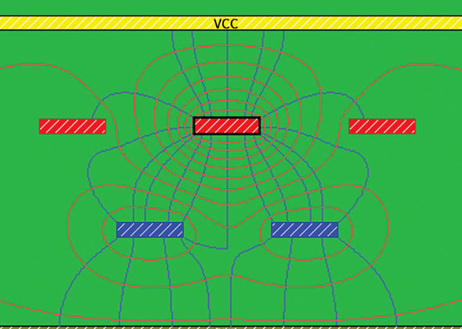
Excessive voltage or current affecting one trace can have an adverse effect on another trace, but there is no physical contact between the two traces. This coupling can occur whenever two nets run adjacent to each other for any significant length. When a signal is driven on one of the lines, the electric and magnetic fields it generates can cause unexpected signals to also appear on nearby lines, as shown in the following figure:
Crosstalk occurs when two or more adjacent traces are coupled together
02 Capacitive coupling
The circuit diagram below shows how circuit theory can be used to simulate different types of crosstalk. In this figure, there is some parasitic capacitance between the two traces, which exists due to the broadside coupling between the traces. Because each trace is a conductor loop, each trace acts like an inductor and has some parasitic inductance. Two parallel inductors have a certain mutual inductance, which defines the strength of the inductive coupling between the two traces.
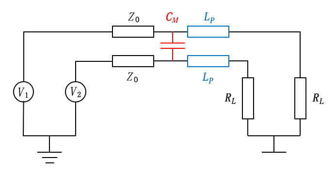
Circuit diagram showing classic circuit models describing different types of crosstalk in a PCB
Capacitive coupling means more than just showing the equivalent capacitance created by the edges of traces, although that does contribute to mutual capacitance. The native capacitance of each trace and the broadside capacitance combine to give the total mutual capacitance; they all connect in series and couple back to the ground plane.
When crosstalk occurs and is observed as a snapshot in the time domain, it is difficult to distinguish between the capacitive and inductive contributions to crosstalk.
03 “Aggressor” Signal or Trace Switching
Crosstalk is a particularly difficult phenomenon to predict and control unless it is simulated, because there is almost no way to intuitively know how much crosstalk voltage and current will be generated due to a given coupling.
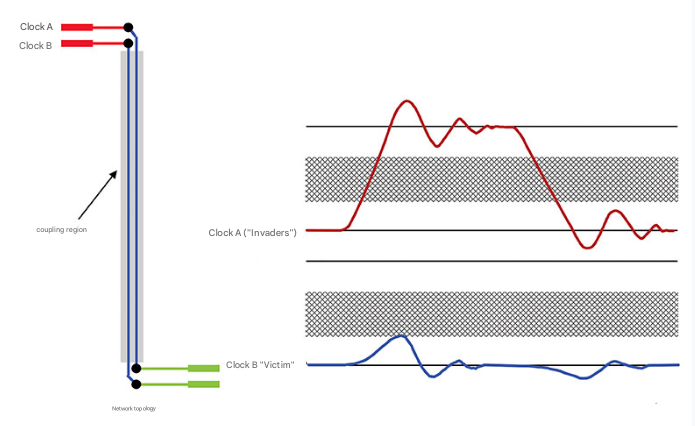
In crosstalk parlance, the “aggressor” signal or trace switches and causes crosstalk. The “victim” signal or trace responds by creating an unexpected signal. The effect is inherently three-dimensional. The victim can be adjacent on the same layer, or above or below the aggressor (below).
The victim network can be located above, below, or near the attacker network
04 Forward and backward crosstalk
In reality, there are two coupled signals added to the victim network: a forward signal and a backward signal. The “forward” pulse propagates with the interfering signal, while the “backward” pulse returns from the interfering signal. The crosstalk at the far end of the victim is called “far-end crosstalk” or FEXT, and the coupled voltage at the near end is called “near-end crosstalk” (NEXT). The figure below shows forward and backward crosstalk.
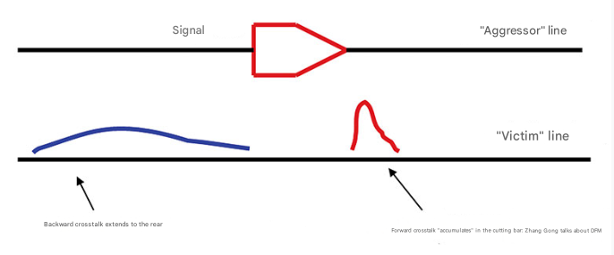
Schematic diagram of forward and backward crosstalk on the victim trace
3. Causes of crosstalk
01 Capacitive and inductive coupling
Capacitive coupling is due to parasitic capacitance, while inductive coupling is due to mutual inductance.
02 Difference in propagation speed
Difference in propagation speed, possible crosstalk
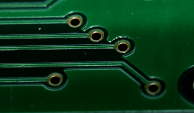
03 PCB vias
PCB vias with stubs can produce reflections, which can cause ringing, which can cause crosstalk.
04 Increased data rate
As data rates increase, rise times also increase. According to Faraday’s law, as rise times increase, crosstalk also increases.
05 Board size
As PCB board size increases, trace lengths also increase, and these traces act like antennas.
4. Tips for reducing crosstalk in PCB design
01 Check key networks close to I/O networks
It is important to review the routing of key networks associated with I/O lines because noise can easily leave or enter the board through these I/O lines (as shown below) and couple the PCB to the outside world or to other PCBs or modules in the system.
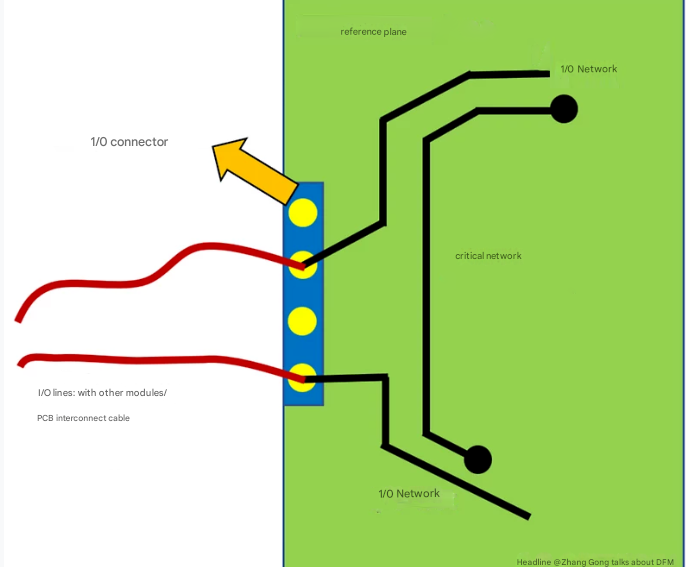
Schematic diagram of a scenario where critical nets and I/O nets are routed close to each other
Any noise that enters the board through the I/O lines has the potential to couple to the critical nets that carry important data/clock signals, which is essentially the immunity aspect of the PCB (left in the image below). In a similar way, any high-speed signal carried by the critical net can couple to the I/O nets, ultimately reaching the outside world through the I/O lines coming out of the board and into other modules in the system. In principle, this would be the emissions aspect of the PCB (right in the image below).
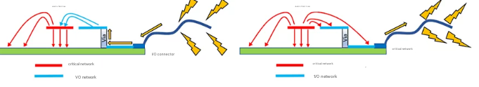
Potential EMI/EMC issues caused by proximity of critical nets and I/O nets
02 Minimum width between traces
When defining the PCB layout, some rules can be set in the CAD tool used, such as the minimum distance between two traces and the minimum distance between each trace and the components present on the board. Different distance values can also be set related to specific netlists or the area in which the netlist will be routed.
PCB design software applications usually include functions that can specify the width and distance of differential signal pairs, or on which PCB layers the netlist can be routed and the preferred direction that the traces can take.
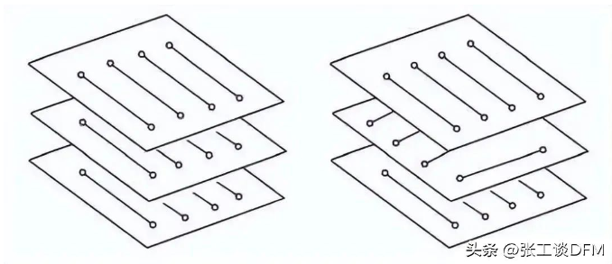
03 Keep traces on adjacent layers perpendicular
PCB layers should be configured so that signals passing through adjacent layers have mutually perpendicular directions, and it is absolutely avoided that their traces are parallel. It is also said that if the traces on one layer are “from north to south”, then the traces on the layer next to it should be “from east to west”. This simple precaution allows you to minimize the effects of broadside coupling.
This is shown in the figure below: on the left is a layout to avoid, on the right is a layout to apply.
04 Use a ground plane
Between two adjacent signal layers, it is best to insert a ground plane (or, a power plane), which further reduces the possibility of broadside coupling.
This solution has the dual advantage of increasing the distance between the layers and providing a better ground return path for the signal layer. In the figure below, we can see a classic four-layer PCB divided into two signal layers (outer), an inner layer for the ground layer (0V) and an inner layer for the power supply.
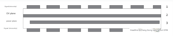
Multilayer PCB Example
05 Utilizing Ground Return Paths
Although it contradicts what was said earlier, an alternative technique that can be used to reduce crosstalk is precisely to exploit the parallelism that exists between traces and couple the ground return path with the high-frequency signal.
In fact, since the ground return path has the same amplitude but opposite direction relative to the signal, it can cancel the effect and thus reduce crosstalk.
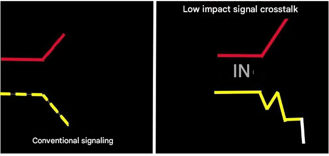
06 Use differential signaling
Another way to ensure signal integrity and minimize the effects of crosstalk is to use differential signaling, that is, two signal lines with the same amplitude but opposite polarity form a single high-speed signal. Since the signal is obtained as the difference in voltage between the two signal lines when receiving, and since electromagnetic noise affects both lines equally.
Therefore, the signal can maintain a high degree of integrity even in the presence of significant external noise. The recommendation is to keep as much distance as possible between the differential signal pair and other PCB traces. The rule of thumb is to choose a distance of at least three times the track width.
07 Reduce the width of parallel traces
In all cases where parallelism between traces cannot be avoided, it is necessary to ensure that their width is as short as possible to reduce the degree of coupling.
PCB with traces
08 Isolate high-frequency signals from other traces
High-frequency signals (such as clocks) must be as far away as possible from traces carrying other signals. Even in this case, the rule of thumb can be applied to choose a minimum distance equal to three times the trace width.
Crosstalk affects signal transmission
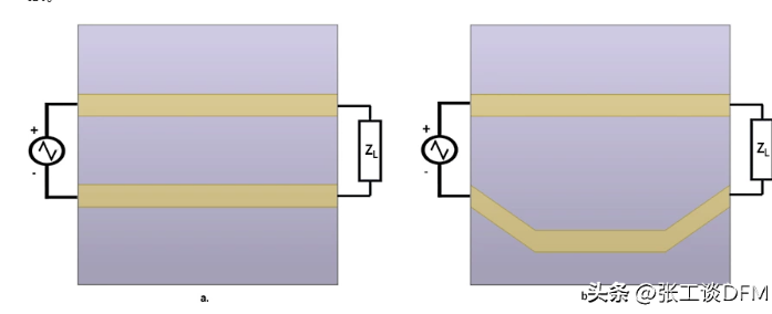
09 Keep exposed critical trace lengths as short as possible
On high-speed PCBs (> 100MHz) with shorter wavelengths, the electrical length of any critical net (see the left figure below) is sufficient to make it an efficient radiator, especially when exposed on the top or bottom layers. This unwanted radiation can couple to any adjacent traces or even to cables present in components close to the traces.
It is recommended to bury the critical nets between solid planes on the inner layers of the PCB, as shown in the right figure below. This helps control the fields in the traces and avoid any unintentional coupling in the form of crosstalk or EMI. If exposing the critical net is unavoidable, keep the length of the exposed portion as short as possible. This is because shorter lengths of exposed traces will have a lesser tendency to radiate, as they would be inefficient antennas if their electrical size were small.
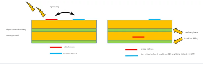
Illustration of exposing or burying critical nets between solid planes
10 Isolate asynchronous signals
Asynchronous signals, such as reset or interrupt lines, should use routing that is as far away from high-frequency signals as possible. Asynchronous signals are often placed near power lines or signals that control switches because these signals are only used during certain phases of the circuit operation and not continuously.
11 Backdrill vias
Via stubs degrade signal integrity and therefore increase crosstalk, which can be reduced by implementing backdrilling.
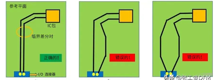
12 Select differential pair routing
Tightly coupled differential routing eliminates crosstalk because noise from an interfering source is equally coupled into both legs of the differential pair, creating common-mode noise. Differential pair suppression helps reduce common-mode noise from crosstalk.
In theory, differential pairs carry signals of equal magnitude but opposite polarity because the EMI generated by the signals cancels or can be ignored. However, this only works if the traces in the pair are equal length and as close to each other as symmetrically as possible.
Violating any of these will create common-mode noise and EMI issues, especially for differential networks carrying high-frequency critical signals, because EMI increases the frequency of the signals being carried.
The following figure shows a few examples of the right/wrong way to route critical differential pairs between the IC package and the exit point (connector) on the board.
Return current paths when there is a split reference plane
Matching critical differential networks: simulation and relationship to actual test requirements
In the PCB example below, there is a simple differential pair routed on the PCB in two different ways: symmetrically and asymmetrically. In both cases, they are excited by a differential voltage source on one end and terminated by a load on the other end.
Example of a differential pair routed on a PCB
13 Using guard traces
Guard traces are used to control capacitive crosstalk between transmission lines. However, they should be used with caution because using guard traces can affect