PCB signal integrity is not handled? Teach you how to make high-speed signals jump over PCB traces
Every time the serial data rate increases, it exposes problems that are masked at lower speeds. Many of these problems are caused by the degradation of signal integrity caused by losses in PCB traces, vias, and connectors. Although there are many solutions to signal integrity problems, each solution has its own disadvantages. One response to these problems is to use cable accessories instead of PCB traces.
Every time the serial data rate increases, it exposes problems that are masked at lower speeds. Many of these problems are caused by the degradation of signal integrity caused by losses in PCB traces, vias, and connectors. Although there are many solutions to signal integrity problems, each solution has its own disadvantages. One response to these problems is to use cable accessories instead of PCB traces.
Here’s the problem. The circuit boards used in servers and switches are typically large, and they are generally equipped with “out-of-the-box” I/O copper or optical fiber on one end and backplane connections on the other end. In order to minimize the total distance the signal travels, PCB designers place the switching IC (FPGA or ASIC) approximately in the center of the board. Of course, placing I/O and switching components close together can minimize signal losses between them, but this can make signal integrity from the ASIC or FPGA to the backplane even worse.
With today’s baseband signal frequencies at 14 GHz, losses due to skin effect, weaving, surface roughness, vias, and connectors are often too great to prevent reliable communication. Even if a receiver can detect an incoming signal 38 dB below the transmitter’s amplitude, the signal degradation is often unacceptable.
28 Gb/s non-return-to-zero (NRZ) signaling is clocked at 14 GHz. To help reduce signal losses at 56 Gb/s, many engineers turn to four-level pulse amplitude modulation (PAM4)—which doubles the data rate for a given signal rate compared to NRZ. Thus, 56 Gb/s can be achieved with PAM4 signaling at a 14 GHz clock rate, but there is a problem. The amplitude (eye height) of a PAM4 signal is only one-third that of an NRZ signal (Figure 1). So there is a trade-off between signal loss and sensitivity to noise.
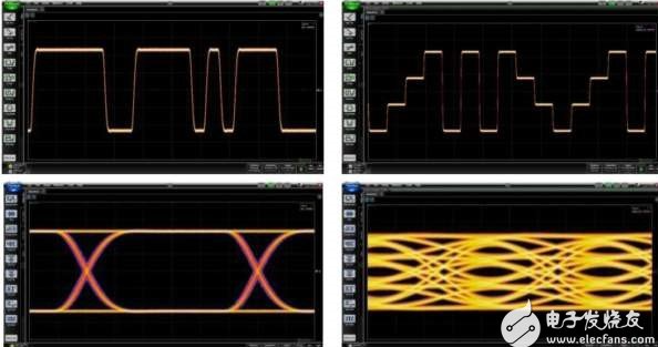
Figure 1: The eye opening of a PAM4 signal (right) is about one-third the height of an NRZ signal, making it more susceptible to noise and errors.
Scott McMorrow, CTO of Samtec’s Signal Integrity Division, provides a spreadsheet that tabulates and graphs the difference in loss (dB) for Megtron6 PCB material and cable sizes from 28 AWG to 36 AWG at different lengths and frequencies from 1 GHz to 50 GHz. Distances include 1 inch, 12 inches, and 1 meter. You can use this data to estimate the signal loss for a specific design.
To mitigate PCB loss issues, several connector companies, including Molex, Samtec, and TE Connectivity, have developed interconnects that allow signals to bypass PCB traces. These cable assemblies come in many varieties, depending on the application. For example, they connect I/O (usually optical modules such as QSFP) to ASICs, ASICs to backplanes, and board-to-board, replacing rigid backplanes and chip-to-chip connections on the same board. Figure 2 shows an example of a jumper cable from a demonstration at DesignCon 2017.
Figure 2: Jumper cable accessories allow signals to bypass the PCB between an I/O connector and an ASIC or FPGA. Samtec offers straight or right-angle connectors.
“Using cables to route 56Gb/s signals reduces losses by about half compared to using PCB traces,” said Nathan Tracy, system architecture group expert and manager of industrial standards at TE Connectivity. Figure 3 compares the losses of several PCB materials and two cable sizes at different frequencies. As you might imagine, the thicker 30 AWG wire has less loss than the 34 AWG wire. But there is a downside to lower loss, warns Greg Walz, advanced technology marketing manager at Molex. Lower-loss wires have lower reflection rejection than higher-loss wires, and increased reflections raise the noise floor, which is critical for PAM4 encoding, especially on shorter cable lengths. So you still need to balance loss with reflections and noise.
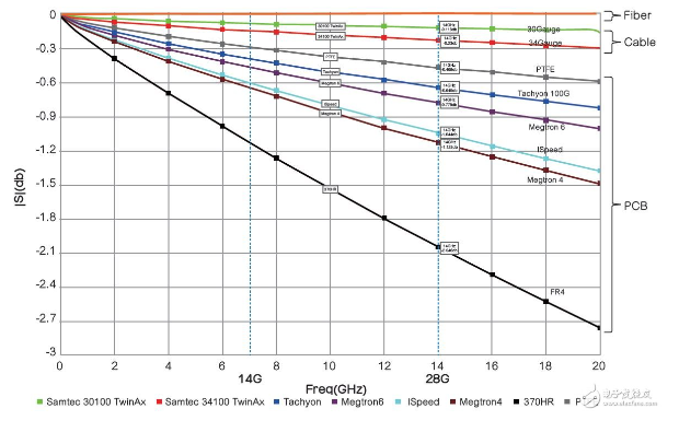
Figure 3: Use this table to compare the loss values of PCB materials and conductors at different frequencies.
Cable accessories used to bypass PCB traces have many names, such as Sliver, Firefly and BiPass. This article refers to such products as “jumper” accessories. Jumpers are made with straight and right-angle connectors that are connected together by a series of differential pairs commonly called “twinax”. Figure 4 shows Samtec’s Eyespeed high-performance twinax cable technology.
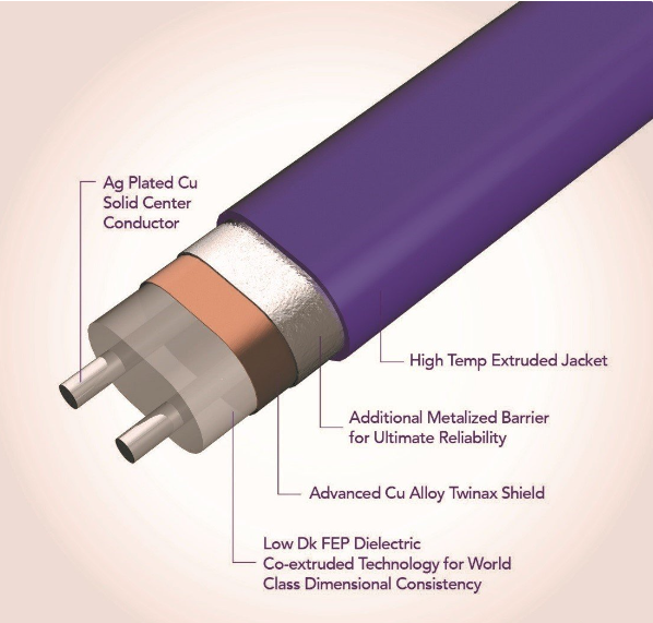
Figure 4: This twinax cable consists of a pair of conductors, a dielectric, two metal shields and a jacket.
It is important to note that the conductors are parallel, not twisted. Twisted pair is usually used for long-distance cables, such as telephone lines. “Twisted pair is suitable for speeds up to about 5Gb/s,” Walz pointed out. Twisting the wires reduces the effects of interference, but at speeds of 28Gb/s NRZ or 56Gb/s PAM4, clock frequencies of at least 14GHz require a pair of parallel shielded wires to mitigate crosstalk issues encountered with twisted pairs. “Twinax cables can attenuate crosstalk by 70dB to 80dB,” Walz added.
There are differences in the construction of these cables. Figure 5 shows a cross-section of a Molex BiPass cable assembly. In addition to the shield, Molex adds a drain wire connected to the reference plane to minimize excess charge inside the cable. Figure 6 shows a cross-section of a twinax cable from TE Connectivity.
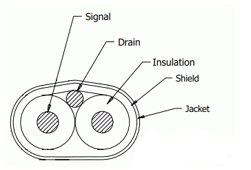
Figure 5: This cross-section shows the twinax wire pairs, shield, and drain wire.
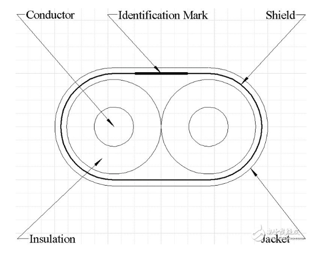
Figure 6: According to TE Connectivity, its twinax cables do not require a drain wire or a second shield.
Because these cables carry signals at very high frequencies, each conductor in a differential pair must be the same length. “Instead of extruding each conductor separately and then fusing them together, both conductors are extruded at the same time under strict process control,” Guetig said. “This ensures that the dielectric constant of the insulating material is consistent.” This consistency minimizes signal skew, a condition that occurs when signals arrive at their endpoints at different times along the pair of conductors. Skew is a serious problem at 14 GHz and higher—a problem that is greatly affected by the conductors passing over or between the fabric weave of the PCB. Therefore, unless the two conductors in a differential trace pass through the same points, there will be skew in the signal. Skew is not a big problem at, say, 10 Gb/s (5 GHz). Jumpers minimize skew because both wires of the differential pair pass through the same material at the same time, unlike the deviation that can occur in PCB traces.
Because these jumpers are cable accessories, they also have connectors. Figure 7 shows some examples of straight and right-angle connectors that can be mounted to the board. Note the shielding for signal integrity. Tracy cautions that cable lengths typically range from about 50cm to 100cm. The cable assembly in the lower right corner of Figure 7 contains eight shielded differential pair cables. Jumpers typically provide multiple sets of eight differential pairs.
Figure 7: Jumpers connect to straight and right-angle connectors that connect to the PCB.
The other end of the cable shown in Figure 6 connects to an optical I/O port such as a QSFP module, but they can also connect to other places on the board through a variety of connectors. The cable assembly shown in Figure 2 has a QSFP module on one end. In this application, the wires in the cable are soldered directly to the QSFP module, so there is no PCB copper trace in the final signal path. The cable can also be plugged directly into the I/O module through a connector. Figure 8 shows how the wires are connected inside the QSFP module. The board connector connects to the board with crimp pins, which separates the control and power pins from the high-speed signals in the cable.
Figure 8: In this configuration, the cable wires are connected directly to the I/O module.
Not all jumper assemblies need to carry signals at data rates of 28Gb/s and higher; they also have applications at lower data rates. For example, storage applications such as hard disk drives and solid-state drives use SATA connections at 6Gb/s and 12Gb/s. For these applications, TE Connectivity offers Sliver cable assemblies that are lower cost than high-speed cables. Figure 9 shows a cable assembly that can carry 56Gb/s signals (top) and an assembly for storage applications.
Figure 9: The cable in the top image is typically used in switches and provides connectivity between optical modules and ASICs or FPGAs. The lower-cost cable (bottom image) is designed for storage applications. Photo taken at the TE Connectivity booth at DesignCon 2017.
Design Tradeoffs
These cable assemblies can improve signal integrity, but they also require tradeoffs for different factors, including cost, flexibility, and heat dissipation. As shown in Figure 3, a 30 AWG wire has lower impedance (and therefore lower loss) than a 34 AWG wire, and better performance can be achieved with a 28 AWG wire. For signal integrity, “bigger is better,” but this comes with a price tag. “Thicker wires are not as flexible as thinner wires, and this can affect board layout because thicker wires are less flexible. The difference in stiffness between a 28 AWG twinax cable and a 34 AWG cable is significant—the 34 AWG cable is very flexible,” said Keith Guetig, product and engineering manager for Samtec’s High-Speed Cable Products Division. Figure 10 shows why flexibility is important, especially in chip-to-chip connections.
Figure 10: Flexibility becomes an important consideration when using high-speed cable assemblies between chips.
Guetig noted that 28 AWG wire can be over 1m long when carrying 28Gb/s NRZ signals, while 34 AWG is typically 50cm or less. He also pointed out that density and flexibility are reasons to use the thinnest AWG wire possible. In addition, using heavier wires will restrict air flow compared to lighter wires.
Thermal issues also play a role in design decisions. Guetig points out that an I/O card used in a network switch might have 40 external connections, each of which requires its own jumper assembly. Adding additional cables for control signals and power means that using jumpers can easily double the number of cable assemblies on the board. This can significantly reduce air flow and make the device hotter. Figure 11 shows the cabling of a 12.8TB/s Ethernet switch with 32 16-difference pair QSFP-DD ports using 34 AWB twinax cables. In this configuration, using thicker wires can reduce air flow to the point where thermal issues become a problem. Each differential pair uses PAM4 to carry 56Gb/s signals.
Figure 11: To keep heat in this Ethernet switch under control, 34 AWG wire is required. Thicker wires would add too much resistance to air flow.
When making design choices, you must consider thermal issues in your thermal budget. Ultimately, you may find that designing the retimer on the board and then just going for the PCB route is a better choice. You must decide on the number of components, signal integrity, cost, and thermal issues in your design. If optical waveguides can be put on PCBs, there will be no need for cables. But it seems that the realization of on-board optical connections will have to wait for another 5 years or more.
Testing cable accessories
Because these jumper accessories need to handle today’s highest-speed signals, you need to know how they will perform in the system. Fortunately, you can use simulation to start the design. Cable suppliers have developed sophisticated test fixtures to characterize these cables. They then measure the characteristics of the cables by de-embedding the fixture effects and then use vector network analyzers (VNAs) to measure the response of these accessories. The supplier will generate the S-parameter files you need for system simulation from the frequency domain measurement data. Then you can use the simulated eye diagram to see the impact of the jumper on signal integrity in the time domain. If you want to verify the simulation by measuring it yourself, you can also request an evaluation board.