How to set jumpers in PCB design
In PCB design, sometimes we will encounter some single-sided boards, that is, the usual single-sided boards (LED-type light boards are more often designed). In this type of board, only single-sided wiring can be used, so jumpers have to be used. Of course, in complex boards, problems that can be solved with jumpers are basically not a problem.
Now let’s talk about how to set jumpers
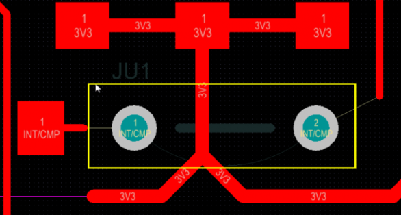
As shown below, this is a board with routing on one side implemented by the jumper designer.
01 Requirements for setting jumpers
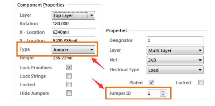
- The component type to be set as a jumper. 2. The jumper IDs of the two plates in the jumper wire component are set to the same non-zero value. Note: Once the component type and pad jumper properties are set, the component will behave as a jumper.
02 How to use jumpers
After completing the above steps, at this stage, there is no automatic network inheritance; after placing a jumper in the work area, you need to manually set the net properties of one of the pads in the pad dialog box.
Note: If a component is defined as a jumper, another pad will automatically inherit the same net name.
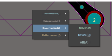
03 Display of jumpers
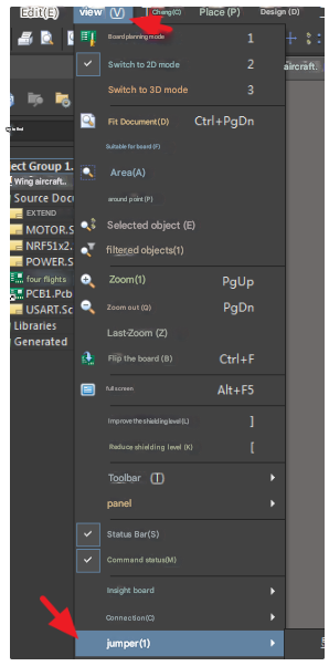
In higher versions of AD, the “View” menu includes a new Jumper submenu that allows control of the display of jumper components. And add a submenu to the Netlist pop-up menu (n shortcut) including options for controlling the display of jumper connection lines. Note: Added a new query keyword Is for filtering and rule definition
Jumper Component
04 Create a jumper footprint in the PCB library
First create a footprint. Typically, jumpers are designed with predefined lengths, such as 0.1 inch (100 milliseconds) increments. As mentioned previously, there are two conditions that must be met: 1. Both pads in the jumper must have the jumper ID set to the same, non-zero value. Note: The pads in all jumper footprints used in the motherboard design have the same jumper ID value. 2. The jumper component must have its type set to jumper. This option can only be set after the Footprint is placed into the PCB workspace, it cannot be set in the PCB
Library Editor.
The figure below is a simple jumper that is 200 mils long;
05 Create a schematic jumper component
- Create a single jumper component, then add all the different length jumper footprints you need. 2. Create a separate jumper component for each different length jumper.
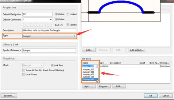
- Once the symbol is created, note: A. Set the default designator, in this case ju? B. Set the component type to Jumper
C. Add the various jumper footprints to the model list as shown above
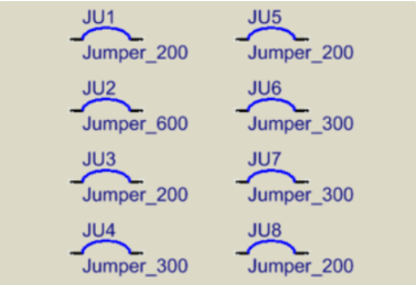
D. Define the other component properties you need, such as a description and any required component parameters. Once you have designed your jumpers, you can place some of them onto the schematic. At this stage, you may not know how many jumpers you will need, but the extras can be easily removed. They are on the schematic to ensure they go in BOOM. As shown below:
06 Position and use of jumpers on PCB
After completing step five, when you select Design » Update PCB
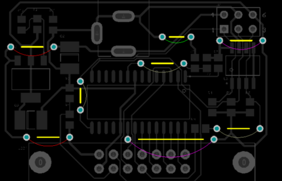
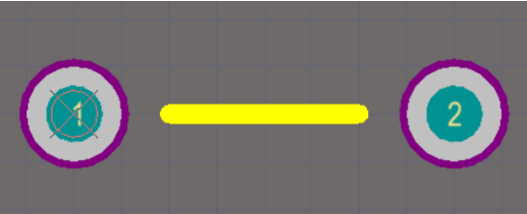
, all jumpers will be placed into the PCB workspace using the default footprint to show the right side of the board shape; the image below shows an almost fully routed pcb, note the remaining connection lines showing where the routing is not completed.
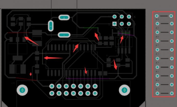
This board is basically wired up, with some connections that cannot be completed because there is no path available in this single-sided design. To complete them, a jumper component will be used.
To complete the connection with a jumper wire:
- Drag the jumper component to the location on the board. If it is not long enough, press the Tab key while moving the jumper, or double-click it after double-clicking it in the Component dialog.
- In the Footprint Name field of the Component dialog, type the desired footprint name, or click the button and select the desired footprint.
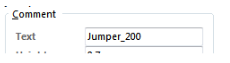
- To make it easier to include the jumper in the BOM, enter a suitable identifying string in the Comment field of the component dialog. In the image below, the footprint name has been copied and pasted into the Comment field, as it describes the length of the jumper.
- Place the jumper in the desired location.
- Double-click to edit one of the pads, and select the desired net name from the Net drop-down list. The other pad in the jumper will automatically be assigned the same net name.
- Once all jumpers are in place, delete any unused jumpers from the board besides them.
- Now run the Design » Update Schematic command to push the footprint and annotation changes back to the schematic.
- The final step is to remove all unused jumper components from the schematic.