Skip to content
Andwin Circuits
  • Home
  • ProductsExpand
    • HDI multilayer PCB
    • Rigid Flex PCB
    • Flex pcb
    • Special PCBExpand
      • High Frequency PCBExpand
        • Rogers RO4350B PCB
        • Rogers RO4003 pcb
        • Rogers RO3003 PCB
        • Rogers 5880 PCB
        • DICLAD 527 PCB
        • Taconic TLX series
        • Taconic TLX-8 RF PCB
        • Taconic TLX-9 RF PCB
      • High speed pcbExpand
        • Megtron 6 High Speed PCB
        • TU-872 SLK Sp High Speed
      • High TG PCBExpand
        • SHENGYI SH260 PCB
        • ISOLA 370HR PCB
        • ISOLA IS410 PCB
        • ISOLA IS420 PCB
      • Heavy copper PCB
      • Copper coin pcb
      • Copper inlay PCB
    • Metal Core PCBExpand
      • Copper core pcb
      • Aluminum PCB
      • 2 Layers Aluminum PCB
      • Direct thermal MCPCB
      • 2 Layers Direct Thermal
    • Ceramic PCBExpand
      • DPC ceramic PCB
      • DBC ceramic PCB
      • Thick film Ceramic PCB
      • Al2O3 Alumina PCB
      • AIN ALN ceramic PCB
      • IGBT Ceramic PCB
  • ServiceExpand
    • PCB Assembly
    • Quick turn PCB assembly
    • PCBA conformal coating
  • IndustryExpand
    • Telecommunication
    • IoT and Wireless
    • Industrial Control
    • Thermal management
    • Power and Energy
    • IC test board
    • Automative
    • Medical
  • CapabilityExpand
    • Rigid PCB
    • Rigid flex PCB
    • Metal core PCB
    • PCB Assembly
  • TechnologyExpand
    • Blogs
    • Via in pad
    • PCB E-test
    • PCB stack up
    • MCPCB panelization
    • Controlled impedance PCB
  • AboutExpand
    • About us
    • Certification
    • Factory Tour
  • Contact
Andwin Circuits
Home / How to associate schematics with PCBs in AD

How to associate schematics with PCBs in AD

ByGrace July 18, 2025July 18, 2025

In Altium Designer (AD for short), associating schematics with PCBs is an important design step that ensures a smooth transition from logical design to physical implementation. The following are the steps to associate schematics with PCBs:

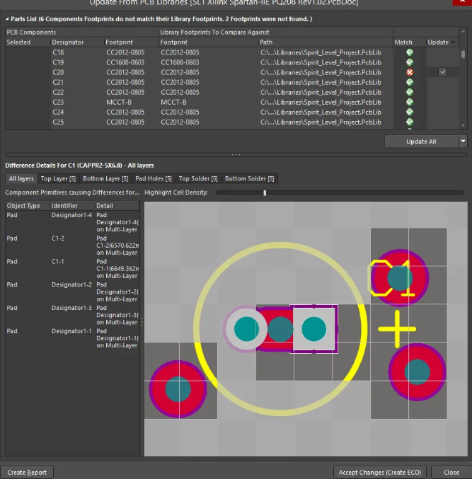
1.Assign component packages


Check and assign packages:

In the schematic, each component needs to have a corresponding PCB package to represent its physical form and pin layout in the PCB design.


Check whether each component in the schematic has been assigned the correct package. If not, you need to assign packages to the components through the library manager or directly from the component library.


Ensure package consistency:


Ensure that the component package in the schematic is exactly the same as the package used in the PCB design, including the number of pins, pin spacing, package size, etc.

Contact us for PCB quote now |

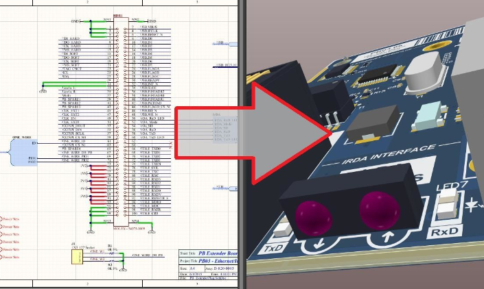
2.Update PCB documents


Perform update operations:


In the schematic editor, click the “Design” option on the menu bar, and then select “Update PCB Document” or a similar option.
In the pop-up dialog box, select the PCB file to be updated and click the “Execute Changes” button.


Observe the import results:

AD will try to synchronize the components and connection information in the schematic to the PCB file. After the import is complete, you can view the results in the PCB editor.

Contact us for PCB quote now |

3.Interactive layout and routing


Use the interactive layout function:

AD provides an interactive layout function that allows users to view the schematic and PCB layout at the same time and interact between the two views.


By placing the schematic and PCB in two windows and setting the interactive mode, you can highlight the corresponding components and connections in the PCB view when clicking on the components in the schematic.


Auxiliary routing:

In the interactive layout mode, users can more intuitively understand the connection relationship between components and perform routing accordingly.
Use the routing tools provided by AD to perform routing according to the design rules to ensure signal integrity and electromagnetic compatibility.

4.Check and optimize


DRC check:

After completing the routing, perform a DRC (Design Rule Check) check to verify whether the PCB design meets all design rule requirements.
Make necessary corrections and optimizations based on the DRC check results.


Optimize layout and routing:

Optimize the layout and routing of the PCB based on the DRC check results and actual needs.
Adjust component positions, rotation angles, and routing paths to improve circuit performance and reliability.

Contact us for PCB quote now |

5.Notes


Ensure software version compatibility:

When designing schematics and PCBs, make sure that the AD software versions used are compatible with each other.


Follow design specifications:

During the design process, follow relevant design specifications and standards to ensure the correctness and reliability of the design.


Back up important files:

Before performing important operations, be sure to back up schematic and PCB files to prevent data loss or damage.

Contact us for PCB quote now |

    Post Tags: #aluminum clad pcb#aluminum core pcb#aluminum pcb#assemble pcb#pcb design

    Post navigation

    Previous Previous
    Contents of PCB manufacturability design review
    NextContinue
    The Relationship Between Layout and PCB in Electronic Design

    Search

    Search

    Products

    • HDI Multilayer PCB
    • Rigid Flex PCB
    • Flex pcb
    • High Frequency PCB
    • High speed pcb
    • Heavy copper PCB
    • Metal Core PCB
    • Ceramic PCB

    Address

    Andwin Circuits Co.,Limited
    Email: sales@andwinpcb.com
    Tel: +86 755 2832 9394
    Fax:+86 755 2992  6717
    ADD:1-2F-1217,HouDeQun Industrial park,
    NanTing RD NO.56,ShaJing,BaoAn,Shenzhen 518104,GuangDong,China

    Products

    • HDI Multilayer PCB
    • Rigid Flex PCB
    • Flex pcb
    • High Frequency PCB
    • High speed pcb
    • Heavy copper PCB
    • Metal Core PCB
    • Ceramic PCB

    Technology

    • Blogs
    • Via in pad
    • PCB E-test
    • PCB stack up
    • Metal core PCB panelization
    • Controlled impedance PCB

    CERTIFICATION

    Certification >>


    Copyright© 2003 - 2026 Andwin | All Rights Reserved | Powered by Andwin

    Scroll to top
    • Home
    • Products
      • HDI multilayer PCB
      • Rigid Flex PCB
      • Flex pcb
      • Special PCB
        • High Frequency PCB
          • Rogers RO4350B PCB
          • Rogers RO4003 pcb
          • Rogers RO3003 PCB
          • Rogers 5880 PCB
          • DICLAD 527 PCB
          • Taconic TLX series
          • Taconic TLX-8 RF PCB
          • Taconic TLX-9 RF PCB
        • High speed pcb
          • Megtron 6 High Speed PCB
          • TU-872 SLK Sp High Speed
        • High TG PCB
          • SHENGYI SH260 PCB
          • ISOLA 370HR PCB
          • ISOLA IS410 PCB
          • ISOLA IS420 PCB
        • Heavy copper PCB
        • Copper coin pcb
        • Copper inlay PCB
      • Metal Core PCB
        • Copper core pcb
        • Aluminum PCB
        • 2 Layers Aluminum PCB
        • Direct thermal MCPCB
        • 2 Layers Direct Thermal
      • Ceramic PCB
        • DPC ceramic PCB
        • DBC ceramic PCB
        • Thick film Ceramic PCB
        • Al2O3 Alumina PCB
        • AIN ALN ceramic PCB
        • IGBT Ceramic PCB
    • Service
      • PCB Assembly
      • Quick turn PCB assembly
      • PCBA conformal coating
    • Industry
      • Telecommunication
      • IoT and Wireless
      • Industrial Control
      • Thermal management
      • Power and Energy
      • IC test board
      • Automative
      • Medical
    • Capability
      • Rigid PCB
      • Rigid flex PCB
      • Metal core PCB
      • PCB Assembly
    • Technology
      • Blogs
      • Via in pad
      • PCB E-test
      • PCB stack up
      • MCPCB panelization
      • Controlled impedance PCB
    • About
      • About us
      • Certification
      • Factory Tour
    • Contact
    Search