Common PCB layout problems and confusions
In electronic design, after the project schematic design is completed and compiled, the PCB design needs to be carried out. After the board size, stacking design, and overall partition conception are determined, the first step of the design is to place the components in their appropriate positions. The layout is a crucial link. The quality of the layout directly affects the wiring effect, thereby affecting the entire design function. Therefore, a reasonable and effective layout is the first step to a successful PCB design.
Before PCB layout, the circuit is partitioned by module according to the entire function. When planning the area, the analog part and the digital part are isolated according to the function, and the high-frequency circuit is isolated from the low-frequency circuit. After the partition is completed, consider the key components in each area, and place other components in the area in the appropriate position with the key components as the focus. When placing components, consider the internal circuit routing between subsystem circuits, especially the timing and oscillation circuits. In order to eliminate potential problems of electromagnetic interference, the component placement and layout should be systematically checked to facilitate routing, reduce electromagnetic interference, and try to be beautiful while meeting the function.
1.Common PCB layout issues and confusions
The success of a product requires good functional quality on the one hand and beautiful appearance on the other. You should lay out your circuit board like carving a piece of craftwork. There are often these questions and troubles in PCB component layout.
Does the PCB shape match the whole machine? Is the spacing between components reasonable? Are there any horizontal or height conflicts?
Does the PCB need to be assembled, do you need to reserve process edges, do you need to reserve installation holes, and how to arrange positioning holes?
How to consider impedance control, signal integrity, power signal stability, and power module heat dissipation?
Are components that need to be replaced frequently easy to replace, and are adjustable components easy to adjust?
Is the distance between thermistors and heating components considered?
The EMC performance of the whole board, how to layout can effectively enhance anti-interference ability?
2.Excellent PCB component layout principles
First, divide the area. According to the functional units of the circuit, consider all the components of the circuit as a whole, divide the functional circuit units into general areas according to the modules, make the layout suitable for signal flow, and try to keep the direction consistent.
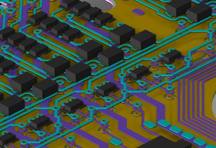
As shown in the figure above, the general functional modules include power supply, core control, signal input processing, signal output processing, connector, human-computer interaction, etc. The module area needs to be divided according to the actual function of the circuit board. The general principle is that the power supply is concentrated on the edge of the board, the core control is in the middle of the board, the signal input is on the left of the core control, and the signal output is on the right of the core control. The connector is arranged on the edge of the board as much as possible, and the human-computer interaction should be reasonably laid out considering the requirements of human-machine engineering. Under the premise of ensuring electrical performance, the components of each functional module should be placed on the grid and arranged parallel or vertically to each other for neatness and beauty.
Then, the core components of each functional module circuit are taken as the center and the layout is carried out around this center. The components should be arranged evenly, integrally and compactly on the PCB, and the leads and connections between the components should be minimized and shortened to facilitate wiring and reduce electromagnetic interference. In PCB, special components such as power devices, adjustable devices, heat-generating and heat-sensitive devices, key components of high-frequency parts, core chips, components susceptible to interference, devices with large volume or weight, devices with high voltage, and some heterogeneous components, the location of these special components needs to be carefully analyzed, and the layout must meet the requirements of circuit functions and production needs. Inappropriate layout may cause circuit compatibility problems and signal integrity problems, thus leading to the failure of PCB design. The location of special components should generally follow the following principles when laying out:
DC/DC converters, switching elements and rectifiers should be placed as close to the transformer as possible, and rectifier diodes should be placed as close to the voltage regulator and filter capacitor as possible. To reduce the length of their lines.
Electromagnetic interference (EMI) filters should be as close to EMI sources as possible. Shorten the connection between high-frequency components as much as possible, and try to reduce their distributed parameters and mutual electromagnetic interference. Susceptible components should not be too close to each other, and inputs and outputs should be as far away as possible.
The layout of adjustable components such as potentiometers, adjustable inductance coils, variable capacitors, and micro switches should take into account the structural requirements of the entire spanner. Some frequently used switches should be placed where they are easily accessible to the hand if the structure allows. The layout of components should be balanced and dense.
Heating components should be arranged at the edge of the PCB to facilitate heat dissipation. If the PCB is installed vertically, the heating components should be arranged above the PCB. Thermistors should be kept away from heating components.
When laying out the power supply, try to make the device layout convenient for the power line routing. When laying out, it is necessary to consider reducing the area of the input power loop. When meeting the flow requirements, avoid running the input power line all over the board and the area of the loop being too large. The good coordination of the positions of the power line and the ground line can reduce the impact of electromagnetic interference. If the power line and the ground line are not properly coordinated, many loops will appear and noise may be generated.
Due to the different frequencies, the interference and interference suppression methods of high and low frequency circuits are also different. Therefore, when laying out components, digital circuits, analog circuits, and power circuits should be laid out separately by module. Effectively isolate high-frequency circuits from low-frequency circuits, or divide them into small sub-circuit module boards, which are connected with connectors.
In addition, special attention should be paid to the distribution of components for strong and weak signals and the direction and path of signal transmission in the layout. In order to minimize interference, after the analog circuit part and the digital circuit part are separated, high, medium and low-speed logic circuits should also be kept in different areas on the PCB. The PCB board is divided according to frequency and current switching characteristics. Noise components should be farther away from non-noise components. Thermistors should be farther away from heating components. Low-level signal channels should be away from high-level signal channels and unfiltered power lines. Separate low-level analog circuits from digital circuits to avoid common impedance coupling between analog circuits, digital circuits and power supply common return lines.
3.Tips for component layout
Switch the application of various grids in PCB component placement;
Application of component alignment tools. Various intelligent alignment methods help you easily locate;
Intelligent placement of components, highlighting prompts, component exchange (Smart placement);
Global batch editing to modify the properties of components and various objects, making your changes more convenient;
3D intelligent real-time display to detect the matching of components inside the PCB board and the whole machine outside the board.