How to Create PCB Fabrication Drawings in Draftsman
Drawing panel fabrication drawings is an integral step in the process of making PCBs. Fabrication drawings for individual PCBs only show the drill holes and board features for a single PCB, but these need to be combined into one drawing for the entire panel. Depending on the specific needs of each company or manufacturer, some design teams will need to take over the creation of panel drawings, including specifying the method of depaneling and the arrangement of the boards in the panel.
If your design team will be creating the panels, you have a full set of native design tools at your disposal in Altium Designer. Another option is to export the panel drawings to another program (most commonly AutoCAD) to complete the panel in a custom format or merge it with other data such as mechanical drawings. Here’s how you can create your drawing format in Altium Designer and export the required panel drawings.
Getting Started with Panel Fabrication Drawings
In this article, I’ll show an example project provided by Zach Peterson. The project is an LED connector board that gives a good overview of the panel fabrication drawing creation process.
Before you start creating your panels, you should answer some important questions:
How do you plan to depanel the PCB?
What panel sizes does your manufacturer support?
Do they specify tool hole and v-groove cut requirements?
Do the panels require datum points?
If tab routing is used in the panel, what are the tool dimensions?
If you can get this information, then you will have enough data to start creating your own panels.
Start with an Embedded Board Array
Inside Altium Designer, the main tool we want to use to create panels is the Embedded Board Array. This gives you a starting board arrangement to which you can start adding tool holes, dimensions, datum points, layer number etching and silkscreen markings.
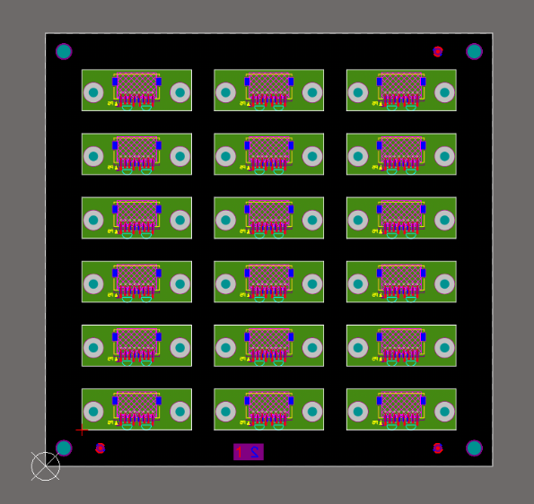
Once the Embedded Board Array object is placed in the PCB Editor, you can add the locations of any mouse bites or v-grooves in the PCB panel. Placing mouse bites involves placing cutouts in the panel and drawing drill points in the remaining tab area that connects the board. This is discussed in this article.
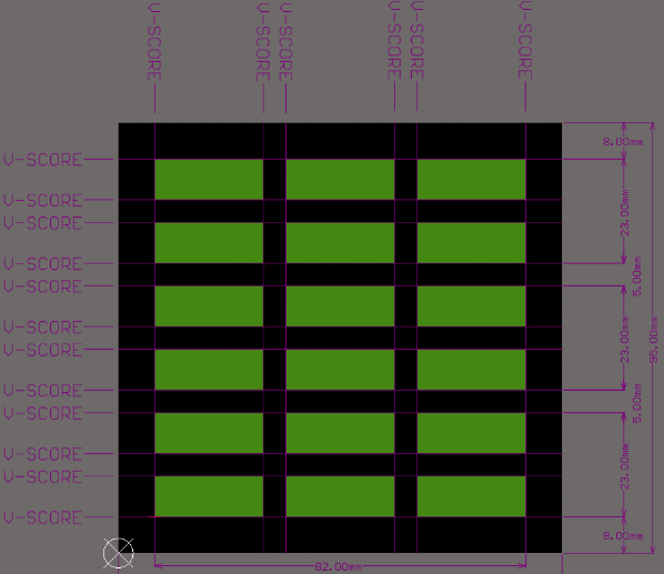
In the example above, we will add v-shaped cutouts to the PCB to indicate the board split lines. Note that the V-marks require some clearance around the tool to allow for the size of the V-marker and copper clearance around the board outline. In the example above, there are no plane layers or copper pours, so there will be plenty of clearance for nearby copper or components.
The V-marks are marked in the Mechanical layer as shown below. As we will see later, it may be useful to copy this to the Drill layer.
This completes the manufacturing nature of the panel, as the drill holes for the PCB and tool will automatically populate on the Drill layer. Some manufacturers provide templates (as DXF or DWG files) that can be used to create panel drawings like the one shown above, and imported into the Mechanical layer to get started.
Creating a Panel Drawing in Draftsman
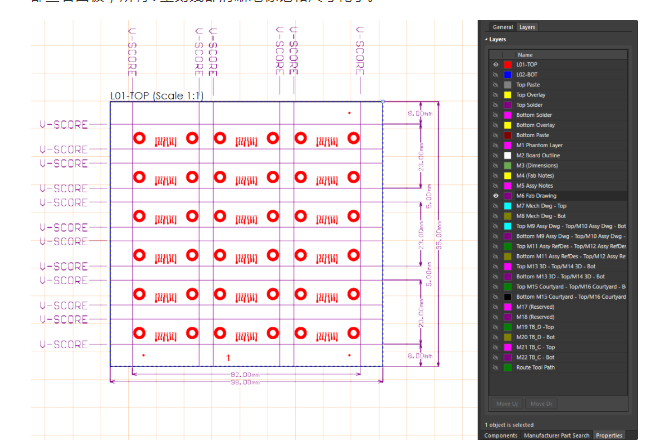
Draftsman treats PCB panels the same as any other PCB, and a variety of views can be imported into a Draftsman drawing. This includes the standard Drill Plan view, which shows the drill symbols for manufacturing, as well as Drill Tables, Assembly Views, Fabrication Views, etc.
To get the dimensioned V-lines into the panel fabrication drawing, you can use a Sheet Fabrication View. This will force the V-lines to be displayed in an isolated view, while the top layer is still visible. To do this, place a Fabrication View in the Draftsman document, and enable the Fab Drawing layer. This will show the V-lines and copper in the top etch layer. Now it is clear that you are viewing the panel from the top, and all the V-lines are clearly labeled and dimensioned.
Other features you’ll want to include in your PCB panel fabrication drawings include:
Stackup drawings showing layers, thicknesses, Dk values or product names and Gerber layer extensions
Fabrication instructions detailing how the board is built and meets standards
Drill table with clearly labeled drill symbols and tolerances
Title block with project information, company information and traceability documentation
Any information about controlled impedance requirements for each layer
If you want a comprehensive drill view of your PCB panel features, it can be helpful to copy the dimensions and V-marks to the Drill Sheet layer. This way, you can use the Mechanical layer in the PCB Editor to create everything for your panel fabrication drawings.
Do it all in the PCB Editor
If you prefer not to use Draftsman, or prefer to do all your design work within a unified interface, you can draw your panel fabrication drawings directly in the PCB Editor. To do this, you can apply drawing blocks, panel fabrication annotations, stackup drawings, etc. to the Mechanical layer and toggle these elements to be visible in the PCB. Once completed, there is the option to export the results as a consolidated DXF file. This is still common practice for many companies, and DXF export still allows other disciplines to work within a standard file containing the PCB data.
Whether you need to build reliable power electronics or advanced digital systems, you can use the full PCB design capabilities and world-class CAD tools in Altium Designer. To enable collaboration in today’s interdisciplinary environment, innovative companies are using Altium 365 to easily share design data and move projects into production