The relationship between wiring spacing and voltage
In pcb design,voltage is a one of vital parameters.High voltage may cause arc discharge corona,electric coupling and interference between circuits,and the wiring spacing between circuits is an important factor in determining voltage distribution.This article will elaborate on the relationship between pcb wiring spacing and voltage,and explore the importance of wiring spacing in pcb design.
Definition and significance of PCB wiring spacing
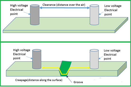
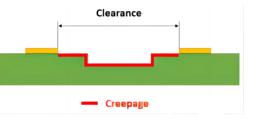
PCB wiring spacing refers to the distance between two electrical components, wires or electrical connections on a circuit board. Usually, the wiring spacing is given by PCB design specifications or manufacturing standards to ensure that the electric coupling and interference between circuits are minimized. The purpose of wiring spacing is to prevent arc discharge or corona and reduce interference between circuits.
Relationship between wiring spacing and voltage
Electric field strength: The wiring spacing determines the intensity distribution of the electric field, thereby affecting the distribution of voltage. When the wiring spacing is small, the electric field strength is high, which may cause partial discharge or breakdown. On the contrary, when the wiring spacing is large, the electric field strength is low, which can reduce the generation of electric coupling and interference.
Capacitance effect: The wiring spacing also affects the capacitance effect between components. When the wiring spacing is small, the capacitance value is large, which will lead to longer charging and discharging time of the capacitor, thereby increasing the circuit response time. Large wiring spacing can reduce the capacitance value and improve the response speed of the circuit.
Inductance effect: The wiring spacing will also affect the inductance. Especially in high-frequency circuits, the inductance is very sensitive. Smaller wiring spacing will increase the crosstalk and mutual inductance of the circuit, thereby affecting the voltage stability and the quality of signal transmission.
Specifications and design practices of wiring spacing
International standards: In PCB design, different countries and regions may have different standards and specifications. Generally speaking, the International Electrotechnical Commission (IEC) gives some minimum standards for PCB wiring spacing in IEC 60950.
PCB manufacturing capabilities: In addition to standard requirements, wiring spacing is also limited by manufacturing processes. Different PCB manufacturers may have different manufacturing capabilities, especially for the minimum wiring spacing requirements. Therefore, when designing PCBs, it is necessary to reasonably select the wiring spacing according to the actual situation.
Strategies for coping with complex wiring: For some complex wiring, such as high-speed circuits and high-frequency circuits, some special wiring techniques and strategies can be adopted to reduce the impact of wiring spacing on voltage to a certain extent. For example, bypass capacitors or impedance matching devices are used to improve the performance of capacitors and inductors.
Design considerations for wiring spacing
Circuit type: Different types of circuits have different requirements for wiring spacing. For example, high-voltage circuits require larger wiring spacing to prevent arc discharge. Low-voltage and high-frequency circuits may require smaller wiring spacing to reduce capacitance, inductance, and crosstalk.
PCB level: In multi-layer PCB design, wiring spacing may also be affected by interference and coupling between different levels. Therefore, it is necessary to select and design wiring spacing according to the hierarchy and wiring level of the PCB.
Temperature: Ambient temperature will also affect the selection of wiring spacing. In a high temperature environment, the dielectric strength and electrical performance of the circuit will be affected, so it is necessary to increase the wiring spacing to improve safety and reliability.
PCB wiring spacing is a very important design parameter, which directly affects the voltage distribution, electrical state density, and the reliability and performance of the circuit. Reasonable wiring spacing design can reduce voltage interference and crosstalk, and improve the working stability and reliability of the PCB. Therefore, when designing PCBs, relevant standard requirements should be followed, and the wiring spacing should be selected and designed in combination with actual conditions. At the same time, different types of circuits and PCB layers also need to consider different wiring spacing to meet specific application requirements.