What is PCB Sandblasting? Understanding the Process and Its Applications
Introduction
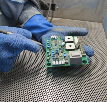
Printed Circuit Boards (PCBs) are essential components in modern electronics, providing the foundation for electrical connections between various components. To ensure optimal performance, PCBs undergo several surface treatment processes, one of which is sandblasting (also known as abrasive blasting). But what exactly is PCB sandblasting, and why is it used?
This article explores the purpose of PCB sandblasting, its benefits, the different techniques involved, and its applications in the electronics manufacturing industry.
What is PCB Sandblasting?
PCB sandblasting is a surface preparation technique that involves propelling fine abrasive particles at high speed onto the PCB surface to clean, roughen, or modify its texture. This process helps in:
- Removing contaminants (such as oxidation, residues, or solder mask imperfections).
- Improving adhesion for coatings, solder masks, or conformal coatings.
- Enhancing surface roughness to promote better bonding in multilayer PCBs.
- Deburring and smoothing edges after mechanical cutting or drilling.
Unlike chemical etching, sandblasting is a mechanical process that does not involve harsh chemicals, making it an environmentally friendly option for PCB surface treatment.
How Does PCB Sandblasting Work?
The sandblasting process for PCBs typically involves the following steps:
- Abrasive Selection:
- Common abrasives include aluminum oxide, glass beads, silicon carbide, or plastic media.
- The choice depends on the desired surface finish and PCB material.
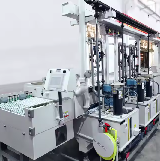
- Blasting Equipment:
- A sandblasting machine directs the abrasive media at the PCB surface using compressed air.
- The pressure, nozzle distance, and blasting angle are carefully controlled.
- Surface Treatment:
- The abrasive particles impact the PCB, removing unwanted materials or creating micro-roughness.
- The process can be adjusted for light cleaning or aggressive surface modification.
- Post-Blasting Cleaning:
- After sandblasting, PCBs are cleaned to remove residual abrasive particles.
- Techniques include ultrasonic cleaning, brushing, or compressed air blowing.
Key Benefits of PCB Sandblasting
1. Improved Adhesion for Coatings
- Sandblasting creates a microscopically rough surface, enhancing the bonding of solder masks, conformal coatings, and plating layers.
2. Oxide and Contaminant Removal
- Effectively eliminates oxidation, flux residues, and other impurities that could affect soldering or electrical performance.
3. No Chemical Waste
- Unlike chemical etching, sandblasting does not produce hazardous waste, making it a greener alternative.
4. Precision and Control
- The process can be finely tuned to avoid damaging delicate PCB traces while still achieving the desired surface finish.
5. Deburring and Edge Smoothing
- Helps remove sharp edges or burrs left after mechanical PCB cutting or drilling, reducing the risk of short circuits.
Types of Abrasive Media Used in PCB Sandblasting
Different abrasives produce varying surface effects:
| Abrasive Type | Characteristics | Best For |
|---|---|---|
| Aluminum Oxide | Hard, sharp, long-lasting | Heavy cleaning, surface roughening |
| Glass Beads | Smooth, round, less aggressive | Gentle cleaning, matte finish |
| Silicon Carbide | Extremely hard, fast cutting | Precision etching, deep cleaning |
| Plastic Media | Soft, non-damaging to delicate surfaces | Light cleaning, conformal coating prep |
Applications of PCB Sandblasting
1. Solder Mask Preparation
- Ensures proper adhesion of the solder mask by creating a slightly rough surface.
2. Multilayer PCB Fabrication
- Improves bonding between layers by increasing surface roughness before lamination.
3. Removing Conformal Coatings
- Helps strip old coatings for rework or repair without damaging underlying circuits.
4. High-Frequency PCB Manufacturing
- Enhances plating adhesion for RF and microwave PCBs, where signal integrity is critical.
5. Rework and Repair
- Cleans oxidized or contaminated pads before re-soldering components.
Limitations and Considerations
While PCB sandblasting offers many advantages, there are some challenges:
- Potential for Over-Etching: Excessive blasting can damage thin copper traces.
- Abrasive Residue: Proper cleaning is required to prevent particle contamination.
- Not Suitable for All PCBs: Flexible PCBs or those with very fine traces may require gentler methods.
Conclusion
PCB sandblasting is a versatile and effective surface treatment method that enhances PCB performance by improving adhesion, removing contaminants, and ensuring a clean surface for further processing. By selecting the right abrasive media and optimizing blasting parameters, manufacturers can achieve high-quality PCB finishes without relying on harsh chemicals.
As electronics continue to evolve, sandblasting remains a valuable technique in PCB fabrication, repair, and surface preparation—ensuring reliability and longevity in electronic devices.