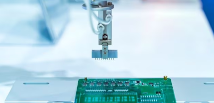
Laboratory fast PCB manufacturing method
Printed circuit boards (PCBs) are the basic components of electronic components, and PCB manufacturing is a basic experimental skill for electronic majors and electronic engineers. Although PCB board manufacturing technology has developed maturely enough, it is unrealistic and unnecessary to produce circuit boards that meet professional PCB manufacturing processes if they just want to prove their designs, because it is time-consuming and costly. Therefore, this article will provide a simple method to produce double-sided PCBs so that electronic majors and engineers can have a better alternative.
Laboratory fast PCB manufacturing method
There are two main methods for PCB manufacturing: chemical mode and physical mode. Nowadays, the most popular PCB manufacturing methods in high schools are thermal transfer and physical engraving. The former belongs to the field of chemistry, and the latter belongs to the field of physics.
Thermal transfer printing
For thermal transfer, first an ordinary laser printer is used to print the PCB image onto a special thermal transfer paper. Then, the PCB image that has been printed on the thermal transfer paper is transferred to the copper clad laminate (CCL) by a thermal transfer device. Finally, a high-precision PCB is produced after subsequent processes (including etching and PCB drilling). In high school laboratories, thermal transfer printing can be used to produce high-precision PCBs and can be completed within an hour. When it comes to double-sided PCB manufacturing, the outstanding problem lies in the misalignment that has not been successfully solved using current manufacturing methods. Therefore, double-sided PCBs manufactured using the thermal transfer method cannot achieve optimal work on electronic products.
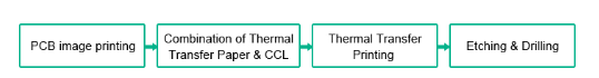
Thermal transfer printing adheres to the following PCB manufacturing process:
- The bottom PCB image is printed on a piece of thermal transfer paper by an ordinary laser printer.
- The top PCB image is printed on another piece of thermal transfer paper by an ordinary laser printer.
- Two pieces of thermal transfer paper are tightly attached to the well-cut double-sided CCL. Transparent tape can be used to fix the position of the paper and the printing plate to avoid misalignment.
- Thermal transfer printing is performed by sticking the CCL with thermal transfer paper in the thermal transfer equipment. Then the CCL printed with the PCB image is obtained after cooling.
- Etching and PCB drilling are then implemented.
The process can be summarized as the following figure:
Laboratory rapid PCB manufacturing method
In all stages of thermal transfer printing for PCB manufacturing, the application of step 3 can accurately lead to the alignment of two sheets of thermal transfer paper. However, when it comes to step 4, misalignment is often caused in the thermal transfer equipment. Therefore, double-sided PCBs are difficult to successfully manufacture unless several trials are carried out.
Physical engraving
According to the basic principle of physical engraving, physical engraving conforms to the principle of milling, milling away the extra or unnecessary parts of the CCL. The application equipment is actually a small CNC drilling and milling machine, also known as a circuit board engraving machine. In the process of double-sided PCB manufacturing, after one side of the milling is completed, the board should be flipped over to mill on the other side of the board. The flipping process may cause misalignment, which should be corrected by software and hardware to reduce the scrap rate of double-sided PCBs.
Comparison of thermal transfer and physical engraving
According to the comparison of the two methods, thermal transfer performs better than physical engraving in the following aspects:
1. CNC drilling and milling machines have higher costs and occupy more laboratory space. However, thermal transfer machines have the characteristics of low cost and small space occupation compared to CNC drilling and milling machines.
- When using thermal transfer printing, double-sided PCBs can be completed within one hour. Although there may be misalignment of multiple thermal transfer printings, double-sided PCBs can be manufactured in up to 3 hours. However, CNC drilling and milling machines require more time, at least 4 hours. In addition, CNC drilling and milling machines can only process one PCB board at a time, while thermal transfer is able to produce multiple double-sided PCBs in the same time.
An improved thermal transfer method
In order to solve the prominent misalignment problem in traditional thermal transfer, this article will provide an improved thermal transfer method for PCB manufacturing, the following steps.
- The bottom PCB image and the mirror PCB image are printed on the same thermal transfer paper, and the holes of the bottom PCB image and the top PCB image are linearly symmetrical.
- The thermal transfer paper is folded along the symmetry line and covered on the well-cut double-sided CCL.
- The double-sided CCL with thermal transfer paper is then placed in the thermal transfer printing equipment for thermal transfer. The folded part first enters the thermal transfer equipment, and after cooling, the CCL printed with the PCB image can be obtained. Etching and PCB drilling.
By printing the top and bottom PCB images on the same thermal transfer paper, the above process can effectively solve the misalignment problem in traditional thermal transfer printing for PCB manufacturing. Therefore, reliable double-sided PCBs can be manufactured smoothly at one time.
PCB image printing on the same thermal transfer paper can be based on any holding different PCB design software to complete the operation. In summary, this improved PCB manufacturing thermal transfer printing method is the most effective for electronic professionals or engineers who can be used in the laboratory to produce double-sided PCBs.