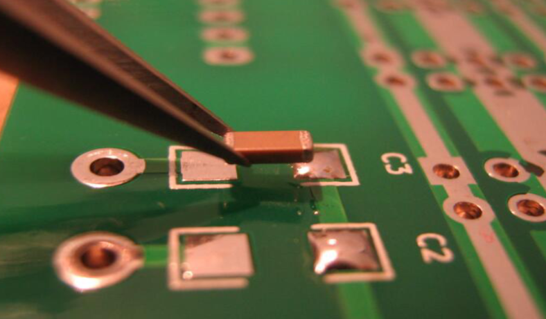
Can the PCB pad area be soldered?
In the field of electronic manufacturing, PCB (printed circuit board) is an indispensable part of electronic equipment. The convexity problem of the PCB pad area may affect the welding quality and the reliability of the circuit board.
1.Causes of PCB pad area convexity
1.1 Material problem
One of the main reasons for the PCB pad area convexity is material problems. If the material quality of the PCB substrate is poor or it is damaged during the production process, it may cause convexity in the pad area. In addition, the thermal expansion coefficient of the pad material does not match the thermal expansion coefficient of the substrate material, which may also cause convexity in the pad area.
1.2 Production process problems
Production process problems are also an important reason for the PCB pad area convexity. During the PCB production process, if the plating thickness of the pad is uneven or the aperture of the pad is too large, it may cause convexity in the pad area. In addition, environmental factors such as temperature and humidity during the production process will also affect the convexity of the pad area.
1.3 Design problems
PCB design problems may also cause convexity in the pad area. If the pad design is unreasonable, such as the distance between the pad and the wire is too close, or the shape of the pad is irregular, it may cause the pad area to bulge.
2.The impact of the convexity of the PCB pad area
2.1 Welding quality problem
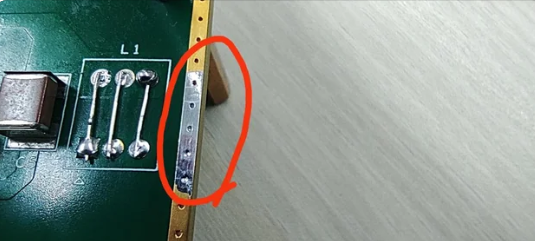
The convexity of the PCB pad area will affect the welding quality. The convex pad may cause the solder to be not evenly distributed on the pad, thus affecting the firmness and electrical performance of the welding. In addition, the convex pad may also cause solder bridging, further affecting the welding quality.
2.2 Circuit board reliability problem
The convexity of the PCB pad area will also affect the reliability of the circuit board. The convex pad may cause the circuit board to be more easily damaged when it is impacted by external force. In addition, the convex pad may also cause the circuit board to be more prone to failure in harsh environments such as high temperature and high humidity.
2.3 Production efficiency problem
The convexity of the PCB pad area will also affect the production efficiency. During the welding process, the convex pad may cause the welding equipment to not work properly, thereby reducing production efficiency. In addition, the convex pad may also lead to an increase in defective welding products, further affecting production efficiency.
3.Solutions to the convexity of PCB pad area
3.1 Material selection and control
Selecting high-quality PCB substrate materials and pad materials is the key to solving the convexity problem in the pad area. In the material selection process, pad materials with thermal expansion coefficients that match the substrate materials should be selected to reduce the convexity of the pad area. In addition, the quality of the materials should be strictly controlled to avoid the use of inferior materials.
3.2 Production process optimization
Optimizing the production process is an effective means to solve the convexity problem in the PCB pad area. In the production process, the plating thickness and aperture of the pad should be strictly controlled to reduce the convexity in the pad area. In addition, the production environment should be optimized, such as controlling temperature, humidity, etc., to reduce the convexity in the pad area.
3.3 Design optimization
Optimizing PCB design is also an important measure to solve the convexity problem in the pad area. In the design process, the distance between the pad and the wire should be reasonably set to avoid irregular pad shapes. In addition, the thermal expansion coefficient of the pad should also be considered to reduce the convexity in the pad area.
3.4 Welding process improvement
Improving the welding process is the key to solving the convexity problem in the PCB pad area. During the welding process, appropriate welding temperature and welding time should be selected to reduce the convexity in the pad area. In addition, suitable welding equipment and welding materials should be selected to improve the welding quality.
3.5 Quality inspection and control
Strengthening quality inspection and control is an effective means to solve the convexity problem in the PCB pad area. During the production process, the PCB pad area should be inspected regularly and problems should be adjusted in time. In addition, a complete quality management system should be established to ensure that the quality of the PCB pad area is effectively controlled.
4. Conclusion
The impact of the convexity problem in the PCB pad area on the electronic manufacturing industry cannot be ignored. Through material selection and control, production process optimization, design optimization, welding process improvement, quality inspection and control, etc., the convexity problem in the PCB pad area can be effectively solved and the reliability and production efficiency of electronic equipment can be improved.