High-Speed and High-Density PCB: Challenges and Solutions for Radiated Emissions
Abstract
This paper examines the growing challenges of radiated emissions (RE) in high-speed, high-density printed circuit boards (PCBs) that are fundamental to modern electronics. As signal speeds exceed GHz frequencies and component densities reach unprecedented levels, traditional PCB design approaches struggle to contain electromagnetic interference (EMI). This article analyzes the root causes of RE in advanced PCBs, explores measurement and simulation techniques, and presents comprehensive mitigation strategies including innovative stackup designs, advanced materials, and layout optimization methods. The discussion incorporates recent industry developments such as ultra-low-loss dielectrics, embedded passives, and 3D packaging technologies that are reshaping EMI control paradigms.
1. Introduction
The relentless advancement of electronic systems has pushed PCB technology into regimes where signal integrity (SI), power integrity (PI), and electromagnetic compatibility (EMC) concerns converge. Modern high-performance computing, 5G infrastructure, and automotive electronics demand PCBs handling multi-gigabit data rates (often exceeding 112 Gbps in cutting-edge designs) while accommodating thousands of interconnections within shrinking form factors. This technological evolution has made radiated emissions (RE) control exponentially more challenging, with traditional design rules becoming inadequate at these extreme operating conditions.
Industry data reveals that 60-70% of EMC certification failures now originate from PCB-related RE issues, costing developers significant time and resources for redesigns. The Federal Communications Commission (FCC) and international standards like CISPR 32 continue to lower emission limits, creating stringent requirements that demand sophisticated design approaches. This paper systematically addresses these challenges by examining emission mechanisms, analysis methodologies, and innovative solutions for next-generation PCB designs.
2. Fundamental RE Mechanisms in High-Speed PCBs
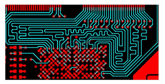
2.1 Common-Mode Radiation from Differential Pairs
While differential signaling theoretically cancels electromagnetic fields, practical imperfections create common-mode currents that radiate efficiently. At 10 Gbps and beyond, imbalances as small as 5% in trace length or 2° in phase can generate significant RE. The radiation efficiency (η) follows:
η ≈ (π * f * I_CM * L_eff * h)^2 / (3 * c^3)
Where f is frequency, I_CM is common-mode current, L_eff is effective antenna length, h is height above reference plane, and c is light speed. In dense PCBs, the proximity effect can increase I_CM by 20-30% compared to isolated traces.
2.2 Power Delivery Network (PDN) Resonances
Modern PCBs contain numerous power domains with decoupling networks forming complex resonant structures. A typical 12-layer board may exhibit 50+ significant resonances between 100 MHz and 10 GHz. When switching currents excite these resonances, the entire PCB can act as a radiating structure. The quality factor (Q) of these resonances often exceeds 20 in high-performance designs, creating narrowband emissions that challenge regulatory limits.
2.3 Via-Related Emissions
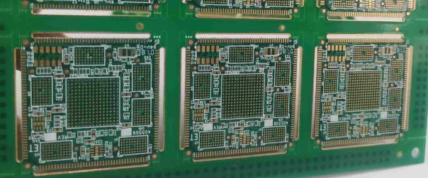
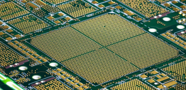
In high-density interconnects (HDI) PCBs with 10+ layers, via transitions become dominant emission sources. A single via passing through a 16-layer board can radiate 15 dB more than its surface trace counterpart at 20 GHz. Stub effects in blind/buried vias create additional resonance points, with the resonant frequency (f_res) approximated by:
f_res ≈ c / (4 * ε_r^0.5 * L_stub)
Where L_stub is the stub length and ε_r is the dielectric constant.
3. Advanced Measurement and Simulation Techniques
3.1 Near-Field Scanning Methodologies
Traditional far-field measurements often miss critical emission mechanisms in dense PCBs. Modern near-field scanners with 100 μm resolution can map EM fields directly above operating boards. Phase-coherent multi-probe systems (8-16 probes) capture time-domain emissions across entire boards, enabling precise localization of emission hotspots. Machine learning algorithms now process this data to predict far-field patterns with 90% accuracy compared to full anechoic chamber measurements.
3.2 3D Electromagnetic Simulation
Full-wave solvers like HFSS and CST have evolved to handle complex PCB geometries. Hierarchical meshing techniques now allow simulation of entire 20-layer boards with 10,000+ vias at frequencies up to 50 GHz. Recent advances in solver algorithms reduce computation time by 40-60% through:
- Domain decomposition methods
- GPU-accelerated matrix solving
- Adaptive frequency sampling
3.2.1 Hybrid Simulation Approach
A practical workflow combines:
- Full-board quasi-static extraction (for power delivery networks)
- Selected 3D full-wave analysis (for critical interconnects)
- Behavioral modeling (for ICs and packages)
This hybrid approach achieves 85-90% correlation with measurements while keeping simulation times practical.
4. Mitigation Strategies for High-Density Designs
4.1 Advanced Stackup Design
Modern high-speed PCBs require carefully engineered layer stacks incorporating:
4.1.1 Ultra-Thin Dielectrics
Core thicknesses below 50 μm reduce loop areas but require careful attention to manufacturing tolerances. The optimal thickness (d) between power/ground layers follows:
d ≤ λ_min / (10 * ε_r^0.5)
Where λ_min is the wavelength at the highest frequency of concern.
4.1.2 Hybrid Dielectric Stacks
Combining materials with different ε_r values (e.g., Megtron 6 for signal layers, FR-4 for core) can reduce emissions by 6-8 dB while maintaining cost efficiency. The effective dielectric constant (ε_eff) for mixed-material stacks requires careful modeling.
4.2 Via Optimization Techniques
4.2.1 Anti-Pad Tuning
Precisely shaped anti-pads (oval or slot-shaped) can reduce via capacitance by 30% while maintaining impedance control. The optimal anti-pad diameter (D_anti) relates to via diameter (D_via) as:
D_anti ≈ D_via + 2 * h * tan(θ)
Where h is dielectric thickness and θ is the field spreading angle (typically 45-60°).
4.2.2 Stub Elimination
Advanced back-drilling techniques now achieve stub removal with ±25 μm accuracy, critical for 56+ Gbps designs. Laser microvia drilling allows precise depth control for buried via structures.
4.3 Novel Shielding Approaches
4.3.1 Embedded Electromagnetic Bandgap (EBG) Structures
Periodic structures in power planes create stopbands for surface wave propagation. A typical EBG unit cell size (a) is:
a ≈ λ_g / 2 = c / (2 * f * (ε_eff)^0.5)
Modern designs implement miniaturized EBG cells (2-3 mm pitch) effective up to 15 GHz.
4.3.2 Conformal Shielding
Directly applied conformal shields using silver nanoparticle inks provide 40-50 dB shielding at thicknesses below 50 μm. These are particularly effective for package-on-package configurations common in mobile devices.
5. Emerging Technologies and Future Trends
5.1 Glass Core Substrates
Major manufacturers are transitioning to glass-core PCBs for next-generation packaging. These offer:
- 40% lower dielectric loss at 110 GHz
- Thermal expansion coefficients matching silicon
- Sub-1 μm surface roughness for ultra-low insertion loss
5.2 Active Cancellation Systems
Embedded microcontrollers with RF sensors now implement real-time emission cancellation in high-performance systems. Current implementations achieve 15-20 dB reduction in critical bands with response times under 100 ns.
5.3 AI-Driven Design Optimization
Machine learning models trained on thousands of PCB designs can now predict emission hotspots with 85% accuracy during early layout stages. These tools suggest optimal component placement and routing strategies that reduce RE by 6-10 dB compared to conventional designs.
6. Conclusion
As PCB technology continues advancing toward terabit data rates and 3D system-in-package integration, radiated emission challenges will intensify. Successful designs will require co-optimization of materials, stackup architecture, and layout strategies from the earliest design phases. The industry is transitioning from rule-based design to simulation-driven, AI-assisted approaches that consider RE as a fundamental constraint rather than an afterthought. Future developments in metamaterials, advanced shielding technologies, and active cancellation systems promise to enable next-generation electronics while meeting increasingly stringent EMC requirements.