How Much Do You Know About the Impact of PCB Warpage?
Introduction
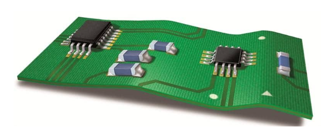
Printed Circuit Boards (PCBs) are the backbone of modern electronics, serving as the foundation for mounting and interconnecting electronic components. One critical yet often overlooked aspect of PCB manufacturing and assembly is warpage—the deformation or bending of the board. PCB warpage can lead to significant issues in assembly, reliability, and performance.
But just how much does PCB warpage affect your electronics? This article explores the causes, consequences, and mitigation strategies for PCB warpage, helping engineers and manufacturers understand its critical impact.
1. What is PCB Warpage?
PCB warpage refers to the undesired bending or twisting of a circuit board, which deviates from its intended flatness. Warpage can occur during manufacturing, assembly, or even in operation due to thermal and mechanical stresses.
Types of Warpage:
- Global Warpage: The entire board bends like a dome or a saddle.
- Local Warpage: Only a specific section of the PCB deforms, often near high-stress areas.
Industry standards (such as IPC-6012 and IPC-A-600) define acceptable warpage limits, typically ≤ 0.75% of the PCB diagonal length for surface-mount technology (SMT) assembly.
2. Causes of PCB Warpage
Several factors contribute to PCB warpage, including:
A. Material Selection
- Uneven CTE (Coefficient of Thermal Expansion): Different layers (e.g., copper, FR4, polyimide) expand at different rates when heated, causing stress.
- Poor-Quality Substrates: Low-Tg (glass transition temperature) materials are more prone to warping under heat.
B. Manufacturing Processes
- Lamination Issues: Improper pressure or temperature during lamination can lead to residual stresses.
- Copper Distribution Imbalance: Uneven copper traces or planes create asymmetric stresses.
C. Thermal and Mechanical Stress
- Reflow Soldering: High temperatures (up to 260°C) can warp thin or improperly designed PCBs.
- Mechanical Handling: Excessive force during drilling, routing, or depaneling induces stress.
D. Environmental Factors
- Moisture Absorption: PCBs stored in humid environments absorb moisture, leading to swelling and warping during reflow.
3. The Impact of PCB Warpage
Warpage affects PCB performance in multiple ways, some of which can lead to catastrophic failures.
A. Solder Joint Defects
- Tombstoning: One end of a component lifts due to uneven solder paste melting.
- Bridging & Open Circuits: Warped boards cause misalignment, leading to solder bridges or incomplete connections.
B. Poor Component Placement
- Misalignment in Pick-and-Place Machines: Warped PCBs cause placement inaccuracies, increasing defects.
- Voiding in BGA Packages: Warpage prevents proper ball-grid-array (BGA) soldering, causing voids and weak joints.
C. Reduced Reliability & Lifespan
- Mechanical Stress on Components: Repeated bending weakens solder joints, leading to cracks over time.
- Thermal Cycling Failures: Warped boards experience higher stress during temperature fluctuations, accelerating failure.
D. Increased Rework & Scrap Rates
- Higher Rejection Rates: Warped PCBs often fail automated optical inspection (AOI), increasing scrap costs.
- Rework Difficulties: Fixing warped boards is time-consuming and may not fully restore functionality.
E. Challenges in High-Density Designs
- Fine-Pitch Components (e.g., 01005 resistors, QFNs): Warpage causes misalignment, making ultra-fine soldering unreliable.
- High-Speed Signal Integrity: Warped traces introduce impedance variations, degrading signal performance.
4. How to Measure PCB Warpage?
Accurate measurement is crucial for quality control. Common methods include:
- Shadow Moiré Technique: Uses light interference patterns to detect warpage.
- Laser Scanning: Non-contact 3D profiling for precise warpage analysis.
- Straightedge & Feeler Gauge: A manual method for quick checks (less precise).
Industry standards recommend measuring warpage at room temperature (25°C), after reflow, and during thermal cycling.
5. Mitigation Strategies for PCB Warpage
A. Design-Level Solutions
✔ Balanced Copper Distribution: Ensure symmetrical copper layers to minimize stress.
✔ Optimal Material Selection: Use high-Tg laminates (e.g., FR4-Tg170) for better thermal stability.
✔ Stiffeners & Support Structures: Add metal or rigid frames to prevent bending.
B. Manufacturing Best Practices
✔ Controlled Lamination Process: Maintain uniform pressure and temperature.
✔ Pre-Baking PCBs: Remove moisture before assembly (typically 2-4 hours at 120°C).
✔ Slow Ramp-Up in Reflow: Reduce thermal shock by gradual heating.
C. Assembly Process Adjustments
✔ Use of Solder Paste with Higher Tack Strength: Prevents component shifting.
✔ Vacuum-Assisted Placement: Ensures components stay aligned on warped boards.
✔ Selective Soldering: Reduces thermal stress on sensitive areas.
D. Post-Assembly Corrections
✔ Mechanical Pressing: Some warped boards can be flattened using controlled pressure (risk of micro-cracks).
✔ Conformal Coating: Adds rigidity to prevent further warpage.
6. Case Study: Warpage in Automotive Electronics
A leading automotive PCB manufacturer faced 15% failure rates due to warpage in engine control modules (ECMs). After analysis, they identified moisture absorption and uneven copper distribution as key causes.
Solution Implemented:
- Switched to high-Tg materials.
- Added pre-baking before assembly.
- Optimized copper balancing in multilayer designs.
Result: Warpage-related defects dropped to <2%, improving reliability and reducing warranty claims.
7. Conclusion: How Critical is PCB Warpage?
PCB warpage is not just a minor manufacturing defect—it can lead to assembly failures, reduced product lifespan, and increased costs. Understanding its causes and implementing preventive measures is essential for high-yield production.
Key Takeaways:
✅ Warpage beyond 0.75% of PCB diagonal length can cause SMT defects.
✅ Material selection, moisture control, and balanced designs are critical.
✅ Advanced measurement techniques help detect warpage early.
✅ Mitigation strategies (thermal management, stiffeners, optimized assembly) reduce risks.
By addressing PCB warpage proactively, manufacturers can enhance product reliability, reduce rework, and ensure smoother production workflows.