The Impact of Chaotic PCB Layout on Component Soldering Quality
Abstract
Printed Circuit Board (PCB) layout design plays a critical role in the manufacturability and reliability of electronic assemblies. A disorganized or poorly planned PCB layout can lead to significant soldering defects, affecting electrical performance, mechanical stability, and long-term durability. This paper examines the key challenges posed by chaotic PCB layouts, including thermal management issues, solder bridging, tombstoning, and void formation. Additionally, it explores best practices for optimizing PCB design to enhance soldering quality and overall product reliability.
1. Introduction
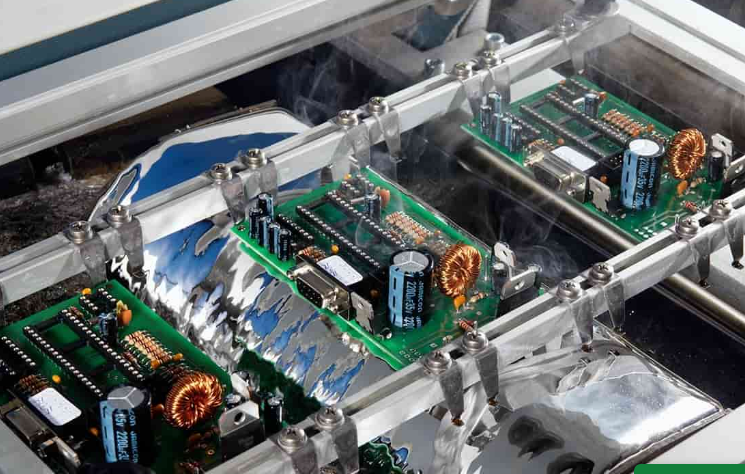
PCB design directly influences the efficiency and quality of the soldering process during surface-mount technology (SMT) or through-hole assembly. A well-structured layout ensures proper heat distribution, minimizes solder defects, and facilitates automated assembly. Conversely, a chaotic PCB layout—characterized by uneven component placement, inadequate spacing, or poor thermal design—can lead to numerous soldering complications.
This article investigates how disorderly PCB arrangements impact soldering outcomes and provides recommendations for mitigating these issues.

2. Key Soldering Challenges Caused by Poor PCB Layout
2.1. Thermal Imbalance and Uneven Soldering
A disorganized PCB layout often results in uneven thermal distribution during reflow soldering. Components with large copper pours or high thermal mass (e.g., ground planes) may heat up slower than smaller components, leading to:
- Cold joints: Insufficient heat prevents proper solder wetting.
- Solder balling: Excessive heat in some areas causes solder splatter.
- Component warping: Differential expansion stresses solder joints.
2.2. Solder Bridging and Short Circuits
Poorly spaced traces or pads increase the risk of solder bridging, where molten solder inadvertently connects adjacent conductors. Common causes include:
- Insufficient pad-to-pad clearance (violating IPC-7351 standards).
- Incorrect solder mask application, exposing copper where it shouldn’t be.
- Improper stencil design, leading to excessive solder paste deposition.
2.3. Tombstoning (Chip Lifting)
Tombstoning occurs when a surface-mount component (e.g., resistors, capacitors) stands vertically due to uneven solder wetting. Chaotic layouts contribute by:
- Asymmetric pad sizes or thermal reliefs, causing unequal heat dissipation.
- Misaligned component footprints, leading to imbalanced surface tension.
2.4. Voids in Solder Joints
Voids (air pockets) weaken solder joints and reduce thermal conductivity. Poor PCB design exacerbates voiding via:
- Trapped flux gases due to inadequate venting in via-in-pad designs.
- Inconsistent pad geometries, hindering uniform reflow.
2.5. Poor Automated Assembly Performance
Automated pick-and-place machines rely on consistent component positioning. A cluttered PCB layout may cause:
- Misaligned placements due to overlapping keep-out zones.
- Insufficient fiducial markers, reducing machine vision accuracy.
3. Best Practices for Optimizing PCB Layout
To mitigate soldering defects, designers should adhere to the following guidelines:
3.1. Thermal Symmetry and Balanced Copper Distribution
- Use thermal relief pads for through-hole components to ensure even heating.
- Avoid large copper fills near small components to prevent thermal shadows.
3.2. Adequate Spacing and Clearance
- Follow IPC-2221/7351 standards for pad spacing and trace widths.
- Implement solder mask dams between fine-pitch components (e.g., QFPs, BGAs).
3.3. Optimized Footprint Design
- Ensure symmetric pad sizes for passive components to prevent tombstoning.
- Use rounded rectangular pads for better solder fillet formation.
3.4. Reflow-Friendly Layouts
- Orient similar components in the same direction to streamline reflow profiles.
- Place heat-sensitive parts (e.g., electrolytic capacitors) away from high-mass areas.
3.5. Design for Manufacturing (DFM) Checks
- Validate layouts using DFM software (e.g., Valor, CAM350) to flag soldering risks.
- Collaborate with assembly partners to refine stencil and reflow parameters.
4. Case Study: Correcting a Chaotic Layout
A case involving a double-sided PCB with frequent solder bridges demonstrated how redesigning the layout resolved issues:
- Problem: Dense QFP packages with 0.5mm pitch caused bridging.
- Solution: Increased pad spacing, added solder mask dams, and adjusted stencil thickness.
- Result: Bridging defects reduced by 85%.
5. Conclusion
A chaotic PCB layout significantly degrades soldering quality, leading to defects that compromise performance and longevity. By prioritizing thermal balance, adequate spacing, and DFM principles, designers can enhance soldering outcomes and reduce rework costs. Proactive collaboration between design and manufacturing teams remains essential for producing reliable PCBs.