PCB Drilling Considerations
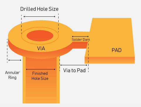
Recent advances in miniaturization have been a major driver of the electronics industry’s continued growth. As miniaturization continues to drive industry growth, manufacturing electronic products and fabricating PCBs are becoming increasingly challenging. The most challenging aspect of PCB manufacturing is the integration of high-density through-holes (VTHs) and interconnects. VTHs are used to mount electronic components that form circuits.
As the density of VTHs increases in PCB assembly lines, the demand for smaller holes also increases. Mechanical drilling and laser drilling are the two primary technologies used to produce holes with precise and repeatable micrometer diameters. Using these PCB drilling technologies, VTHs can range in diameter from 50-300 microns and have depths of approximately 1-3 mm.
Drilling machines consist of a high-speed spindle that rotates at approximately 300k RPM. These speeds are crucial for achieving the precision required for micron-level drilling in PCBs.
To maintain accuracy at high speeds, the spindle utilizes air bearings and a direct drill assembly secured by a precision collet chuck. Additionally, vibration at the drill tip is controlled to within 10 microns. To maintain accurate hole placement on the PCB, the drill head is mounted on a servo stage that controls the stage’s movement in the X and Y axes. A channel actuator controls the PCB’s movement in the Z axis.
As the pitch of holes in PCB assembly lines continues to decrease and the demand for higher throughput increases, the servo control electronics can become outdated. Using laser drilling to create through-holes for PCB manufacturing helps reduce or eliminate this lag, a next-generation requirement.

Laser Drilling
The laser drill head used in the PCB manufacturing process consists of a complex set of optical components that control the laser’s precision required to drill the holes.
The size (diameter) of the hole to be drilled in the PCB is controlled by the aperture, while the hole depth is controlled by the exposure time. Furthermore, the beam is split into multiple energy bands to further enhance control and precision. A moving focusing lens is used to precisely focus the laser beam’s energy at the drilling location. Galveno sensors are used to move and position the PCB with high accuracy and precision. Currently, Galveno sensors capable of switching at speeds of 2400 kHz are used in industry.

Alternatively, a novel method called direct exposure technology can be used to drill holes in circuit boards. This technology, based on image processing, improves accuracy and speed by creating an image of the PCB and converting it into a position map. The position map is then used to align the PCB under the laser during the drilling process.
Advanced research in image processing algorithms and precision optics will further improve the productivity and yield of PCB manufacturing and high-speed drilling used in this process.


