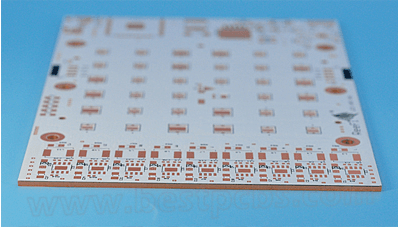
About copper pcb ——Summary of 9 PCB Copper Pour tips
Summary of 9 PCB Copper Pour Tips
I. PCB Copper Pour Tips
- If a PCB has multiple ground planes, such as SGND, AGND, and GND, you should pour copper separately based on their locations on the PCB, using the most important ground plane as a reference. It goes without saying that digital and analog ground planes should be poured separately. Also, before pouring copper, thicken the corresponding power supply lines: 5.0V, 3.3V, and so on. This creates a variety of shapes and shapes.
- For single-point connections between different ground planes, connect them through a 0 ohm resistor, ferrite bead, or inductor.
- For copper pouring around a crystal oscillator: A crystal oscillator in a circuit is a high-frequency radiator. The method is to pour copper around the crystal oscillator and then ground the crystal casing separately.
- For islanding (dead zone) issues, if you think they are significant, simply define a ground via and add it there. This is not a big deal.
- When starting to lay out the wiring, treat the ground trace equally. Route the ground traces carefully during routing. Don’t rely on adding vias after copper is poured to eliminate unconnected ground pins; this will have a negative impact.
- Avoid sharp corners (<=180 degrees) on the board, as this creates a transmitting antenna from an electromagnetic perspective! Other corners will always have some impact, the difference being whether it’s larger or smaller. I recommend using rounded edges.
- Avoid copper plating in open areas of the middle layer of a multilayer board, as it’s difficult to ensure this copper is properly grounded.
- Metal inside the device, such as heat sinks and metal reinforcements, must be properly grounded.
- The heat sink metal block of a three-terminal voltage regulator must be properly grounded. The ground shield near the crystal oscillator must also be properly grounded. In short, properly grounding the copper plating on the PCB will undoubtedly have more benefits than disadvantages. It can reduce the return flow area of the signal line and minimize electromagnetic interference from the signal.
II.PCB Copper Pour Settings
1.PCB Copper Pour Clearance Settings:
The copper pour clearance (clearance) is generally twice the routing clearance. However, if you set the routing clearance for the copper pour before pouring, the subsequent copper pour will default to the routing clearance. This will not produce the desired results.
A simple method is to double the clearance after routing, then pour the copper. After pouring, return the clearance to the routing clearance. This will prevent DRC errors. This method works, but if you need to change the copper pour again, you’ll have to repeat the above steps, which is a bit cumbersome. The best method is to set a separate rule for the copper pour clearance.
Another method is to add a rule. In the Rule Clearance, create a new rule called Clearance1 (the name can be customized). Then, in the Where the First Object matches option box, select Advanced (Query). Click Query Builder. The Build Query from Board dialog box will appear.
In this dialog box, select the default ShowAllLevels from the first drop-down menu. Select ObjectKinds from the drop-down menu under ConditionType/Operator. Select Poly from the drop-down menu under ConditionValue on the right. This will display IsPolygon in the QueryPreview window. Click OK. You’re not done yet; you’ll get an error when you save the full query:
Next, simply change IsPolygon to InPolygon in the FullQuery display window. Finally, modify the copper pour safety clearance to your desired setting within the Constraints. Some people say that routing rules take precedence over copper pours. However, copper pours must adhere to routing safety clearance rules. You need to add this exception to the routing safety clearance rules.
To do this, comment out “notInPolygon” in the FullQuery. This is actually completely unnecessary, as priorities can be changed. In the lower-left corner of the main rule settings page, click “Priorities.” Raise the priority of the copper pour safety clearance rule to a higher priority than the routing safety clearance rule. This will prevent interference. Done!
2. Setting the PCB Copper Pour Line Width:
When selecting either Hatched or None copper pour mode, you’ll notice a field for setting TrackWidth. If you select the default 8mil and the minimum width of the net you’re pouring copper to is larger than 8mil, you’ll get an error during the DRC. I didn’t pay attention to this detail at first, and every copper pour resulted in numerous DRC errors.
To do this, create a new rule called Clearance1 (name it customizable) in the Rule Clearance section. Then, in the Where the First Object matches option box, select Advanced (Query). Click Query Builder. The Build Query from Board dialog box will appear. In the first drop-down menu in this dialog box, select Show All Levels (this option is selected by default).
Then, select ObjectKinds from the drop-down menu under ConditionType/Operator, and then select Poly from the drop-down menu under ConditionVALUE on the right. This will display IsPolygon in the QueryPreview window on the right. Click OK to save and exit. Now, we’re not done yet. Change IsPolygon to InPolygon in the FullQuery window (this fix is necessary due to a bug in DXP; it seems unnecessary in the 2004 version).
This is the final step. Now, you can modify the spacing you need in Constraints (depending on your platemaking process). This will only affect the spacing of the copper layer and will not affect the spacing of the wiring on each layer.