How to prevent sagging and Fracture in flexible PCBs
A flexible circuit board’s neutral bending axis may not be exactly in the center of the circuit stack.Proper handling of flexible circuits can help prevent dents and fractures in flexible PCBs.
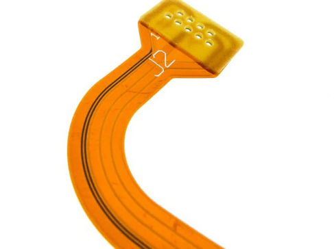
Flexible PCBs are as much mechanical devices as they are electrical devices.The arrangement of conductors should allow the entire circuit to function reliably and adequately.Unlike traditional rigid printed circuit board(rigid PCBs),flexible PCBs can bend,flex,and twist to fit the final assembly,Beyond a certain point this bending can severely strain the circuit,leading to fractures and dents in flexible PCBs.
The flexibility of flexible circuit offers designers a range of options that rigid PCBs lack.Even though flexible circuits are ideal for applications requiring bending and twisting,this doesn’t mean that flexible copper traces will never crack.Like all materials,copper has limits to the type and intensity of stress it can withstand.
This presents various challenges.When dynamic flexing(continuous bending during product use)is required,or in applications where circuits need to be folded into tight spaces within multi-lane enclosures,precision and extreme care must be maintained to avoid fractures.
Considerations for Optimizing Flexing and Bends in Flexible Circuits
Understanding Stress Points and Bend Radius
You need to understand the design issues of bending,folding,and flexing-understand the physics of bending.For single-sided Flex circuits,if extension or compression exceeds the bend radius or stress points,the copper layer will eventually crack.Always ensure you operate within these parameters
Neutral Axis
Foy dynamic flex application,a single-sided(one-layer copper circuits) is recommended.This allows the copper to move in the center of the structure,the copper layer is neither compressed nor tensed during dynamic bending of flexing.
Thinner layer are better
Thinner layer result in smaller inner bend radii,resulting in less stress on the outer layers.For application requiring frequent flexing,thinner copper and thinner dielectric layer are preferred.
I-Beam Design
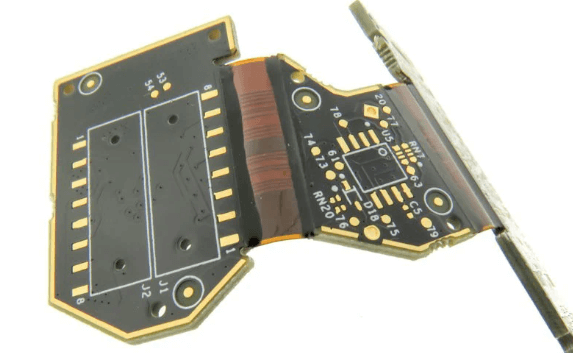
I-Beam construction involves placing the copper or dielectric layer directly on the top of each other.This type of structure becomes more rigid in the folding area.Due to the compression of the inner layers,the outward extension force are significantly increased.To eliminate this issue,the trace on opposite sides should be staggered.
Sharp Bending or Folding
Many flexible circuit boards are folded as part of a design kit.Well-constructed circuits can easily withstand the first fold,twist,or crease.However,wrinkled circuits should not be folded frequently,as the copper will eventually crack.This is not recommended under any circumstances.There are design consideration to avoid this issue,For example,flexible circuit board with rounded traces are designed for this purpose.
Other considerations to avoid trace cracking on flexible circuits include:
Using solder or-solder-coated traces
Using RA(rolled annealed) copper or electrodeposited(ED) copper with a grain orientation
Covering areas of polyimide film that are bent or curved
Using stiffeners on the bottom and coverlay on the top.