Why bake PCBs? How to bake PCBs
1.The primary purpose of baking PCBs is to remove moisture and humidity, removing water vapor trapped within the PCB or absorbed from the outside. This is because some PCB materials are prone to forming water molecules.
In addition, after being manufactured and stored for a period of time, PCBs may also absorb moisture from the environment. Water is one of the main causes of PCB popcorning and delamination. When PCBs are placed in an environment with temperatures exceeding 100°C, such as in reflow ovens, wave soldering ovens, hot air leveling, or hand soldering processes, water turns into water vapor and rapidly expands in volume.
The faster the PCB is heated, the faster the water vapor expands. The higher the temperature, the larger the volume of the water vapor. If the water vapor cannot escape from the PCB immediately, it is likely to cause the PCB to swell.
The Z direction of the PCB is particularly vulnerable. This can sometimes cause the vias between layers to break, sometimes even causing separation between layers. In more serious cases, even blistering, swelling, and cracking can be seen on the PCB’s exterior.
Even if these symptoms aren’t visible on the PCB’s exterior, internal damage is already present. Over time, this can lead to unstable functionality in electrical products or problems like CAF (carbon anode) formation, ultimately causing product failure.
Analysis of the Causes and Prevention of PCB Cracking
The PCB baking process is quite complex. The original packaging must be removed before placing it in the oven. The baking temperature must exceed 100°C, but it must be kept low to prevent excessive expansion of water vapor during baking, potentially causing the PCB to crack.
The industry generally sets the PCB baking temperature at 120±5°C to ensure that moisture is completely eliminated from the PCB before it can be placed on the SMT line and reflowed.
Baking time varies depending on the thickness and size of the PCB. Thinner or larger PCBs should be supported with a heavy object after baking to minimize or prevent the PCB from bending due to stress release during the cooling period after baking.
If the PCB is bent, it can cause offset or uneven solder paste during SMT printing, leading to numerous defects such as short circuits and empty solder joints during reflow.
PCB Baking Conditions
The industry generally sets the following baking conditions and times for PCBs:
- PCBs within two months of the manufacturing date and properly sealed, if unpacked and stored in a temperature and humidity controlled environment (≤30°C/60% RH, per IPC-1601) for more than five days, must be baked at 120±5°C for one hour before being put on the production line.
- PCBs stored for two to six months beyond the manufacturing date must be baked at 120±5°C for two hours before being put on the production line.
- PCBs stored for more than 6-12 months beyond the manufacturing date require a 4-hour bake at 120±5°C before production.
- PCBs stored for more than 12 months beyond the manufacturing date are generally not recommended for use. This is because the bonding strength of multilayer boards deteriorates over time, potentially leading to quality issues such as unstable product functionality and increased returns for market repairs. Furthermore, there are risks of board breakage and solder wicking during the production process. If use is unavoidable, it is recommended to bake them at 120±5°C for 6 hours. Before mass production, test prints of solder paste should be performed on a few boards to ensure there are no solderability issues before continuing production.
Another reason why it is not recommended to use PCBs that have been stored for too long is that the surface treatment will gradually degrade over time. For example, the industry standard shelf life for ENIG is 12 months. After this period, the shelf life depends on the thickness of the immersion gold layer. If the thickness is too thin, the nickel layer may diffuse into the gold layer and cause oxidation, affecting reliability. Caution is essential.
- All baked PCBs must be used within 5 days. Unfinished PCBs must be rebaked at 120±5°C for another hour before being put on the production line.
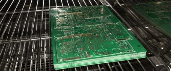
PCB Baking Stacking Methods
- When baking large PCBs, stack them flat. The recommended maximum number of PCBs per stack is 30. Within 10 minutes after baking, remove the PCBs from the oven and lay them flat to cool. After baking, apply a board anti-bend jig. Vertical baking is not recommended for large PCBs, as they are prone to warping.
- When baking small and medium-sized PCBs, stack them flat. The recommended maximum number of PCBs per stack is 40. Alternatively, stack them upright with any number of PCBs. Within 10 minutes after baking, remove the PCBs from the oven and lay them flat to cool. After baking, apply a board anti-bend jig.
PCB Baking Precautions
- The baking temperature must not exceed the PCB’s Tg point, generally not exceeding 125°C. Some early lead-containing PCBs had a relatively low Tg point, while most lead-free PCBs now have a Tg above 150°C.
- Use the baked PCBs as soon as possible. If not, re-vacuum-pack them as soon as possible. If they have been exposed to the workshop for too long, they must be re-baked.
- Remember to install an exhaust drying system in your oven. Otherwise, the water vapor produced during baking will remain inside the oven, increasing the relative humidity and hindering the dehumidification of the PCBs.
- From a quality perspective, the fresher the PCB solder, the better the quality after the oven. Expired PCBs still have some quality risks even if they are baked before use.
Recommendations for PCB Baking
- It is recommended to bake the PCBs at a temperature of 105±5°C. The boiling point of water is 100°C. Above this boiling point, water will turn into water vapor. Since the water molecules in the PCB are relatively small, a high temperature is not required to increase their vaporization rate.
Excessively high temperatures or rapid vaporization can cause water vapor to expand rapidly, which is detrimental to quality. This is especially true for multilayer boards and PCBs with buried vias. 105°C is just above the boiling point of water, yet not too high, allowing for both dehumidification and reducing the risk of oxidation. Furthermore, current oven temperature control capabilities have been significantly improved.
- Whether the PCB needs to be baked depends on whether the packaging is damp. Specifically, check to see if the Humidity Indicator Card (HIC) inside the vacuum packaging indicates moisture. If the packaging is good and the HIC shows no moisture, the PCB can be put online without baking.
- It is recommended to bake the PCB in an upright position with spaced-apart baking trays. This maximizes hot air convection and allows moisture to be baked out more easily. However, for large PCBs, you may need to consider whether an upright baking tray may cause board warping.
- After baking, it is recommended to place the PCB in a dry place and allow it to cool quickly. It is also recommended to place a “board warp prevention jig” on top of the board. Generally, objects tend to absorb moisture more easily during the cooling process from a high temperature. However, rapid cooling can also cause the board to warp. A balance must be struck.
Disadvantages of PCB Baking and Considerations
- Baking accelerates oxidation of the PCB surface coating, and the higher the temperature and the longer the baking time, the more detrimental it is. 2. High-temperature baking is not recommended for boards with an OSP surface treatment, as the OSP film can degrade or even fail due to high temperatures. If baking is unavoidable, it is recommended to bake at 105±5°C for no more than two hours. Use within 24 hours after baking.
- Baking may affect the formation of IMC, especially for boards with HASL (Hydraulic Tin Sintering) and ImSn (Immersion Tin Sintering) surface treatments. This is because the IMC layer (copper-tin compound) is already formed during the PCB stage, before soldering. Baking can increase the thickness of this already formed IMC layer, causing reliability issues.