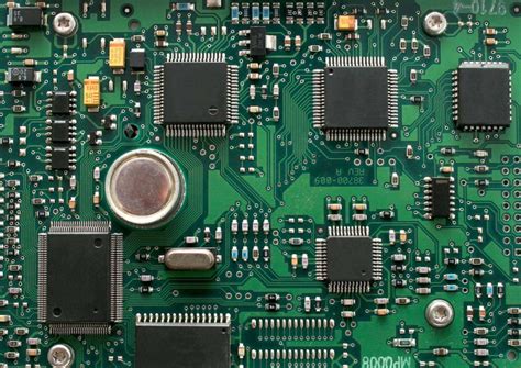
Interference Problem and Solutions for High-Frequency PCBs
In actual research, we have summarized four main sources of interference:power supply noise,transmission line interference,coupling,and electromagnetic interference(EMI).By analyzing various interference issues in high-frequency pcbs and combining them with practical application,we have proposed effrctive solutions.
1.Power Supply Nosie
In high-frequency circuits,power supply noise has a particularly significant impact on high-frequency signals.Therefore,a low-noise power supply is paramount.Here,a clean ground and a clean power supply are equally important.Why?The power supply characteristics are shown in Figure 1.Clearly,the power supply has a certain impedance,and this impedance is distributed across the entire power supply.Therefore,noise is also superimposed on the power supply.Therefore,the power supply impedance should be minimized as much as possible,so dedicated power and ground planes are ideal.In high-frequency circuit design,designing the power supply as a layer is often much better than designing it as a bus.This ensures that the loop always follows the path of minimum impedance.Furthermore,the power supply board must provide a signal path for all signals generated and received on the PCB.This minimizes signal loops and thus reduces noise,a point often overlooked by low-frequency circuit designers.There are several ways to eliminate power supply noise in PCB design.
(1)Pay attention to vias: Vias require etched openings in the power plane to create space for the vias.However,if the opening are too large,they will inevitably affect the signal loop,forcing the signal to detour,increasing the loop area and increasing noise.Furthermore,if several signal lines are concentrated near the opennings and share this loop,the shared impedance will cause crosstalk.
(2)Connecting lines require sufficient ground trace:Each signal should have its own dedicated signal loop,and the loop area of the signal and loop should be as small as possible.In other words,the signal and loop should run in parallel.
(3)Separate analog and digital power supplies:High-frequency devices are generally very sensitive to digital noise,so the two should be separated and connected together at the power supply input.If a signal crosses the analog and digital sections,a loop can be placed at the signal crossing point to reduce the loop area.
(4)Avoid overlapping separate power supplies on different layers:Otherwise,circuit noise can easily couple through parasitic capacitance.
(5)Isolate sensitive components,such as PLLs.
(6)Power Line Placement:To minimize signal loops,place power line next to signal lines to reduce noise.
2.Transmission Lines
Only two types of transmission lines can appear in a PCB: stripline and microwave lines.The biggest problem with transmission lines is reflection,which can cause many problems.For example,the load signal become a superposition of the original signal and the echo signal,increasing the difficulty of signal analysis.Reflection aslo cause return loss,which has the same severe impact on signal generation as additive noise interference:
(1)Signals reflected back to the source increase system noise,making it more difficult for the receiver to distinguish between noise and signal.
(2)Any reflected signal will generally degrade signal quality and change the shape of the input signal.Generally speaking,the solution is impedance matching(for example,the interconnect impedance should closely match the system impedance).However.impedance calculation can sometime be complex;refer to transmission line impedance calculation software.
The following are methods for eliminating transmission line interference in PCB design:
(a)Avoid impedance discontinuities in transmission line.Impedance discontinuities are points where the transmission line changes suddenly,such as straight corners and vias.These should be avoided as much as possible.Methods include:Avoid straight corners in routing,and use 45° angles or arcs whenever possible. Larger angles are also acceptable. Use as few vias as possible, as each via represents an impedance discontinuity. Avoid signals on outer layers from passing through inner layers, and vice versa.
(b)Avoid using stubs.Any stub is a noise source.If the stub is short, it can be terminated at the end of the transmission line.If the stub is long,it will use the main transmission line as the source,generating significant reflections and complicating the problem.Therefore,it is recommended not to use it .
3.Coupling
(1)Common impedance coupling:This is a common coupling channel where the interference source and the interfering device often share certain conductors(such as loop power,bus,common ground,etc.)
(2)Field common-mode coupling cause the radiating source to induce a common-mode voltage in the loop formed by the interfering circuit and on the common reference plane.If the magnetic field dominates,the common mode voltage generated in the series ground loop is Vcm = -(ΔB/Δt) * Area (where ΔB = the change in magnetic induction intensity). If the electromagnetic field is present, given its electric field value, the induced voltage is: Vcm = (LhFE)/48. This formula applies up to L(m) = 150MHz. Above this limit, the calculation of the maximum induced voltage can be simplified to: Vcm = 2h*E.
(3)Differential-mode field coupling:This occurs when direct radiation is sensed and received by a pair of conductors or circuit board leads and their loops.This coupling is greatly reduced if the two conductors are kept as close together,so twisting the two conductors together can reduce interference.
(4)Inter-line coupling(crosstalk)can cause undesirable coupling between any two conductors in a parallel circuit,significantly impairing system performance.It can be categorized as capacitive crosstalk or inductive crosstalk.The former occurs when parasitic capacitance between lines couples noise from the noise source to the noise receiving line through current injection;the latter can be imagined as signal coupling between the imagined as signal coupling between the primary and secondary sides of an undesirable parasitic transformer.The magnitude of inductive crosstalk depends on the proximity of the two loops,the size of the loop area, and the impedance of the affected load.
(5)Power line coupling:This occurs when an AC or DC power line is exposed to electromagnetic interference and then transmits this interference to other devices.
There are several methods for eliminating crosstalk in PCB design:
- Both types of crosstalk increase with increasing load impedance, so signal lines sensitive to crosstalk should be properly terminated.
- Maximizing the distance between signal lines can effectively reduce capacitive crosstalk. This can be achieved by managing ground planes, spacing traces (for example, isolating active signal lines from ground, especially between signal lines undergoing state transitions and ground), and reducing trace inductance. 3. Inserting a ground wire between adjacent signal lines can also effectively reduce capacitive crosstalk. This ground wire should be connected to the ground layer every quarter wavelength.
- For inductive crosstalk, minimize the loop area and, if possible, eliminate it.
- Avoid signal sharing loops.
- Focus on signal integrity: Designers should implement terminations during the soldering process to address signal integrity. Designers using this approach can focus on the length of the microstrip shielding copper foil to achieve good signal integrity performance. For systems with dense connectors in communication structures, designers can use a single PCB for termination.
- Electromagnetic Interference
As speeds increase, EMI becomes increasingly severe and manifests itself in many ways (such as electromagnetic interference at interconnects). High-speed devices are particularly sensitive to this, as they may receive high-speed spurious signals, while low-speed devices may ignore these spurious signals.
There are several methods for eliminating electromagnetic interference in PCB design:
- Reduce loops: Each loop acts as an antenna, so we need to minimize the number of loops, their area, and their antenna effect. Ensure that the signal has only one return path between any two points, avoid artificial loops, and use power planes whenever possible.
- Filtering: Filtering can be used on both power and signal lines to reduce EMI. There are three methods: decoupling capacitors, EMI filters, and magnetic components.
- Shielding. Due to space constraints and the large number of articles discussing shielding, I will not discuss this in detail.
- Minimize the speed of high-frequency components.
- Increasing the dielectric constant of the PCB board can prevent high-frequency components such as transmission lines close to the board from radiating outward. Increasing the thickness of the PCB board and minimizing the thickness of microstrip lines can prevent electromagnetic radiation from leaking outward and also prevent radiation.
Having discussed this, we can summarize the following principles in high-frequency PCB design:
- Unify and stabilize the power and ground planes.
- Carefully considered routing and appropriate terminations can eliminate reflections.
- Carefully considered routing and appropriate terminations can reduce capacitive and inductive crosstalk.
- Noise suppression is necessary to meet EMC requirements.